Tuesday, December 10, 2019

Argonne National Laboratory Installs Forge Nano’s Prometheus ALD tool to enable next gen ALD research and innovation.


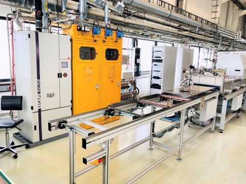
[Press release, Forge Nano, LINK] LOUISVILLE, CO., October 2019 — Delivery and installation of Forge Nano’s industry leading, lab-scale ALD tool- Prometheus has been completed.

Forge Nano’s Prometheus tool is a lab-scale R&D tool designed to make ALD research approachable and affordable. The Prometheus series of ALD tools have been designed to be the world’s most robust, flexible, and economical ALD tools available. Designed with the lab environment in mind, applying nanoscale encapsulating coatings on milligrams to kilograms of powders has never been more attainable. It can also be used to coat small objects.

The Prometheus system accommodates up to 8 precursors, including basic delivery and low vapor pressure delivery draw systems to handle gas, liquid, and solid precursor recipes with ease. (www.foregnano.com)

The U.S. Department of Energy’s Argonne National Laboratory recently commissioned Forge Nano to build and install their revolutionary ALD tool- Prometheus. The Prometheus tool will extend Argonne’s expertise and capabilities to perform a broader range of cutting-edge ALD research on site in a safe, consistent, and reliable manner.

Prometheus features:
  • Largest capacity and throughput. The Prometheus tool is the only commercially available fluidized bed atomic layer deposition (ALD) tool that can process up to 1 kg batches of cathode.
  • Swappable reactor sizes to precisely coat milligrams to kilograms of material
  • Proprietary fluidization aids (jet assist) that enable fluidization and ALD deposition on powders that cannot be successfully and conformally coated on other systems.
  • Inert isolation and handling capabilities of substrates.
  • Proprietary precision-dosing design that allows for higher precision and repeatability of precursor dosing than other equipment on the market
  • Non-discriminant precursor capabilities that allows for precursor types and sizes that other equipment cannot accommodate.

Forge Nano’s is uniquely positioned in the market to enable scale-up from lab to manufacturing so that developed IP has a pathway to commercialization. Our line of tools covers the entire product cycle, from R&D, to pilot scale, to complete manufacturing implementation. Forge Nano’s team of ALD experts guide our customers through the entire process, making ALD feasible for nearly any industry.

“We are excited to see Prometheus installed at Argonne National Laboratory adding to their world-class ALD capabilities. We cannot wait to see the new and exciting innovations that the team at Argonne will develop, using our technology and tools.” –Dr. Paul Lichty

Advanced Energy Announces Grand Opening of State-of-the-Art Advanced Materials Processing Showcase Lab Near Frankfurt

FORT COLLINS, Colo.--(BUSINESS WIRE)--Dec. 10, 2019-- Advanced Energy Industries, Inc. (Nasdaq: AEIS) – a global leader in highly engineered, precision power conversion, measurement and control solutions – is pleased to announce the grand opening of its Advanced Materials Processing (AMP) Showcase Lab near Frankfurt, Germany. Located in Karlstein am Main, the state-of-the-art facility includes office space and lab space for plasma deposition and materials characterization. The lab will serve as a central hub for AE product demonstrations and customers’ plasma deposition research and development activities, providing a superior experience for thin film developers. 
AE’s plasma lab multi-chamber inline coater showing substrate carrier and vacuum load lock in the foreground and with various gas handling cabinets and AE’s power supplies in racks in the background. This equipment includes but is not limited to planar and rotatable dual magnetron sputtering (DMS), and has plasma etch pre-cleaning capability. Various substrate sizes from small experimental coupons (e.g. glass, sapphire, silicon and more) up to 500x600 mm2 rectangular sheets (e.g. glass, plexiglass, plastic, metal and more) can be utilized. (Photo: Business Wire)

Global Semiconductor Equipment Sales Forecast – 2020 Rebound, 2021 Record High

[Press release, Semi, LINK] TOKYO – December 11, 2019 – Global semiconductor manufacturing equipment sales will drop 10.5 percent to $57.6 billion in 2019 from last year’s historic peak of $64.4 billion but stage a 2020 recovery and set a new high in 2021, SEMI, the global industry association representing the electronics manufacturing and design supply chain, reported today in its Year-End Total Equipment Forecast. 


Released at SEMICON Japan 2019, the forecast shows equipment sales registering a 5.5 percent increase to $60.8 billion in 2020 and continued expansion into 2021, with record revenues of $66.8 billion as leading device manufacturesinvest in sub-10nm equipment, especially for foundry and logic.

The SEMI year-end forecast shows sales of wafer fab equipment – consisting of wafer processing, fab facility and mask/reticle equipment – falling 9 percent in 2019 to $49.9 billion. The assembly and packaging equipment segment is on track to decline 26.1 percent to $2.9 billion in 2019, while semiconductor test equipment is forecast to drop 14.0 percent to $4.8 billion this year.

Taiwan will dethrone Korea as the largest equipment market and lead the world with 53.3 percent growth this year, followed by North America with a 33.6 percent uptick. China will maintain the second spot for the second consecutive year, and Korea will fall to third after throttling back capital expenditures. All regions tracked except Taiwan and North America will contract this year.

SEMI expects the 2020 equipment market recovery to be fueled by advanced logic and foundry, new projects in China, and, to a lesser extent, memory. In Europe, equipment sales will surge 45.9 percent to $3.3 billion. Taiwan is forecast to remain the top equipment market next year on the strength of $15.4 billion in sales, with China second at $14.9 billion and Korea third at $10.3 billion. More upside is likely if the macroeconomy improves and trade tensions subside in 2020.

In 2021, all sectors tracked are expected to grow and the memory spending recovery will hit full stride. China is expected to ascend to the top position with equipment sales of more than $16 billion, followed by Korea, and Taiwan.

The Year-End Total Equipment Forecast is based on SEMI's industry-recognized World Fab Forecast database and input from equipment manufacturers. Total equipment includes wafer processing, fab facilities, mask/reticle, total test, and assembly and packaging equipment.

The following results reflect market size in billions of U.S. dollars.

Monday, November 18, 2019

Intel to Reclaim Number One Semiconductor Supplier Ranking in 2019

According to IC Insights, Intel is to reclaim the number one semiconductor supplier ranking in 2019 from Samsung due to the downturn in Memory (DRAM and NAND). The top 3 memory suppliers (Samsung, SK Hynix, and Micron) are according to IC Insights forecast to register ≥29% year-over-year declines in 2018 with SK Hynix expected to decline the most by a 38% down in sales 2019.


The expected top 15 semiconductor (IC and O-S-D—optoelectronic, sensor, and discrete) sales ranking for 2019 is shown above.  It includes six suppliers headquartered in the U.S., three in Europe, two each in South Korea, Japan, and Taiwan.

Source: IC Insights (LINK)

Monday, November 11, 2019

ASM International launches A400(TM) Duo vertical furnace system with dual reactor chambers

New system addresses 200mm applications with high productivity and low cost of ownership

Munich - ASM International N.V. (Euronext Amsterdam: ASM LINK) today introduced the A400™ DUO vertical furnace system with dual reactor chambers for wafer sizes of 200mm and smaller. The system’s DUAL Boat reactors produce high throughput, increasing reactor utilization to a very high percentage, while ensuring low capex.

“The new A400™ DUO reactor ensures that ASM will extend its position as a leader in the market for Power, Analog, RF, and MEMS applications,” said Hichem M’Saad, ASM Executive Vice President, Global Products. “As 200mm manufacturing began its renaissance, driven by growth in for instance IoT devices, it became clear that our existing furnace technology could still achieve industry-leading results. Combining our technology with the latest innovations in robotics and controls has significantly enhanced the system’s manufacturing capabilities to meet today’s production targets.”


The new DUO is compatible with the original A400™, so existing process recipes can be easily transferred, accelerating system ramp. The system has secured production qualification from multiple customers in Europe, the United States and Asia, including several leaders in power, RF, and MEMS device manufacturing. To date over 20 reactors have been shipped, with a healthy outlook for further shipments.

ASM’s original A400™ vertical furnace system has a proven track record of more than 1000 reactors shipped to customers worldwide and over 25 years of maturity in semiconductor manufacturing. The new system has been modernized to support a variety of growing markets including silicon power, wide band gap semiconductor power, analog, RF and MEMS devices. With its updated control system, software with an intuitive graphical user interface, predictive maintenance by advanced control diagnostics, new robot, and plug-and-play installation, customers can count on the A400™ DUO delivering increased reliability with production output that achieves better repeatability, productivity, and time utilization.

Like its predecessor, the A400™ DUO offers a comprehensive portfolio of process applications including low pressure chemical vapor deposition (LPCVD) processes like doped silicon and silicon nitride films, diffusion processes such as wet oxidation and anneal processes.

Sunday, November 3, 2019

Global MEMS and Sensors Fab Capacity to Grow 25 Percent Through 2023, SEMI Reports

MILPITAS, Calif., Oct. 29, 2019 /PRNewswire/ -- Total worldwide installed capacity for MEMS and sensors fabs is forecast to grow 25 percent to 4.7 million wafers* per month from 2018 to 2023, driven by explosive demand across communications, transportation, medical, mobile, industrial and other Internet of Things (IoT) applications, according to the new MEMS & Sensors Fab Report to 2023 published by SEMI.


Listing more than 230 companies with over 400 facilities, the report is the first of its kind focused on MEMS and sensors front end facilities. The report, spanning the 12 years starting in 2012, predicts that MEMS fabs will account for 46 percent of all MEMS and sensors facilities by 2023. Image sensors fabs will represent 40 percent of the total, and other fabs – those producing both MEMS and image sensors – the remaining 14 percent.

Japan led the world in MEMS and sensors capacity in 2018, followed by Taiwan, the Americas, and Europe/Mideast. China is on track to rise from the sixth position this year to the third largest region in installed capacity by 2023. Japan and Taiwan are expected to maintain the top two positions through 2023.

The MEMS and Sensors Fab Report to 2023 shows fab equipment investments hovering at about US$4 billion per year from 2018 to 2023, with most of the spending – an estimated 70 percent – devoted to fabs for image sensors made on 300mm wafer sizes. During the same period, Japan's fab equipment investment is expected to peak at nearly US$2 billion in 2020, with Taiwan topping out at US$1.6 billion in 2023.

All told, 14 new device volume fabs will be added from 2018 to 2023** for MEMS and sensors made on wafers ranging from 8 inches to 12 inches in size. China shows the largest increase in new volume fabs followed by Japan, Taiwan and Europe.

The MEMS & Sensors Fab Report to 2023 includes details on individual fabs such as location, technologies and products, as well as quarterly data from 2012 to 2023 for the following:
Construction and equipment investments
Installed capacities
Wafer sizes
Process nodes

SEMI Industry Research and Statistics developed the MEMS & Sensors Fab Report to 2023 in collaboration with the MEMS & Sensors Industry Group, a SEMI Strategic Association Partner. To learn more about the MEMS & Sensors Fab Report to 2023, click here.

*200mm equivalent capacity – excludes R&D, Pilot and EPI lines
**Excludes R&D, Pilot and EPI lines and fabs with low probabilities of being built

About SEMI

SEMI® connects more than 2,100 member companies and 1.3 million professionals worldwide to advance the technology and business of electronics design and manufacturing. SEMI members are responsible for the innovations in materials, design, equipment, software, devices, and services that enable smarter, faster, more powerful, and more affordable electronic products. Electronic System Design Alliance (ESD Alliance), FlexTech, the Fab Owners Alliance (FOA) and the MEMS & Sensors Industry Group (MSIG) are SEMI Strategic Association Partners, defined communities within SEMI focused on specific technologies. Visit www.semi.org to learn more, contact one of our worldwide offices, and connect with SEMI on LinkedIn and Twitter.

Association Contact

Michael Hall/SEMI
Phone: 1.408.943.7988
Email: mhall@semi.org

Thursday, October 31, 2019

ASM International reports third quarter 2019 results

ASM International N.V. (Euronext Amsterdam: ASM) today reports its third quarter 2019 operating results (unaudited) in accordance with IFRS.

FINANCIAL HIGHLIGHTS
EUR million
Q3 2018
Q2 2019*
Q3 2019
New orders
258.0
373.1
291.8
Net sales
195.7
363.3
271.2
Gross profit margin %
40.9%
59.0%
42.4%
Operating result
28.0
150.2
50.6
Result from investments (excluding amortization intangible assets resulting from the sale of ASMPT stake in 2013)
16.8
2.0
6.5
Amortization intangible assets (resulting from the sale of ASMPT stake in 2013)
(3.1)
(3.4)
(3.5)
Net earnings
39.1
121.6
53.5
Normalized net earnings (excluding amortization intangible assets resulting from the sale of ASMPT stake in 2013 and result from sale of ASMPT shares)
42.2
125.0
56.9
* Including effects of litigation settlement

  • New orders of €292 million driven by foundry and logic, 8% above Q2 2019 (€270 million excluding patent litigation settlement).
  • Net sales for the Q3 2019 were €272 million, 4% up compared to the previous quarter (€260 million excluding patent litigation settlement).
  • Gross profit margin was 42.4% in Q3 2019 compared to 59.0% Q2 2019 (42.8% excluding patent litigation settlement).
  • Operating result of €51 million up €4 million compared to the previous quarter (€47 million excluding patent litigation settlement).
  • Normalized net earnings for the third quarter 2019 decreased by €68 million compared to Q2 2019, excluding the patent litigation settlement net earnings in Q3 showed an increase.

COMMENT

Commenting on the results, Chuck del Prado, President and Chief Executive Officer of ASM International said:

"In Q3 we realized sales of €271 million. Excluding the litigation settlement, this is 4% above the Q2 level, reaching again a new record level, driven by continuous high demand in the logic/foundry segment. Our order intake, at €292 million was well above our guidance of €250-270 million driven by strong pull-ins from our logic/foundry customers. Our cash position in the quarter increased again substantially, partly due to the receipt of 50% of the US$115 million cash proceeds from the litigation settlement."

OUTLOOK

For Q4, on a currency comparable level, we expect sales of €310-330 million while bookings, on a currency comparable level, are expected to be in the range of €290-310 million. This guidance for both sales as well as orders does not include the proceeds of US$61 million related to the settlement of the arbitration proceeding with Kokusai Electric Corporation, which will be added to those numbers in Q4. For 2019, general expectations are now that the wafer fab equipment (WFE) market will decline with a mid-teens percentage. Market demand in the memory segment generally continues to be weak while visibility remains limited. Market demand in the logic and foundry segments is solid in 2019, driven by spending on the most advanced nodes, and expected to continue into the first part of 2020. We expect to strongly outperform the WFE market in 2019.

SHARE BUYBACK PROGRAM

The execution on the €100 million share buyback program, announced on July 23, 2019, will start as from early November.

INTERIM DIVIDEND

ASMI announces today an interim dividend of €1.00 per common share. In view of the recent strong increases in the cash position, the Board decided this year to bring forward part of the 2019 dividend in the form of an interim dividend. The final dividend proposal, which will be in line with ASMI’s policy to pay a sustainable dividend, will be announced as part of the fourth quarter 2019 and full yearresults 2019.

The relevant dates for this interim dividend payment are:

Ex-dividend date share Euronext and OTC US November 5, 2019

Record date November 6, 2019

Payment date November 12, 2019

ARBITRATION SETTLEMENT

As announced on October 29, 2019, ASMI has entered into a settlement agreement with Kokusai Electric Corporation (“KEC”) concerning all the matters of the arbitration proceeding relating to the license agreement which expired in November 2017. KEC will pay an amount of US$61 million to ASM. This settlement of the arbitration proceeding is separate from the settlement of the patents lawsuits and invalidation proceedings as announced on July 1, 2019.

ASM International settles with Kokusai for Batch ALD patent licenses (US$61 million)

October 29, 2019, 12.15 p.m. CET (LINK) ASM International N.V. (Euronext Amsterdam: ASM) today announces that it has entered into a settlement agreement with Kokusai Electric Corporation (formerly known as Hitachi Kokusai Electric Inc. and hereinafter referred to as “KEC”) to resolve the arbitration proceeding relating to the license agreement which expired in November 2017. As part of this settlement, KEC will pay ASM an amount of US$61 million. With this settlement all pending disputes between ASM and KEC with respect to patent licenses have been resolved.

As announced on February 23, 2018, ASM initiated an arbitration proceeding on August 30, 2017 with the American Arbitration Association against KEC for breach of the license agreement between the companies. This license agreement provided KEC and its affiliates a license under certain patents of ASM in the field of Batch ALD. The companies have now entered into a settlement agreement concerning all the matters of the arbitration.

This arbitration settlement is separate from the settlement of all patent lawsuits and invalidation proceedings between ASM and KEC that was announced on July 1, 2019.

The settlement of the arbitration will positively impact ASMI’s sales and bookings in Q4 2019 with an amount of US$61 million, or approximately €56 million.
Background:

- Applied Materials to buy Japan's Kokusai to boost memory chip business and ALD (LINK)

- ASM International settles (US$115 million) with Kokusai Electric Corporation on the use and infringement of ALD patents  (LINK)

Monday, September 30, 2019

Chuck del Prado will step down as CEO of ASM International in May 2020

ASM International N.V. (Euronext Amsterdam: ASM) announces that Mr. Chuck del Prado, Chief Executive Officer, Chairman of the Management Board and President of the company has notified the Supervisory Board that he wishes to retire from the company at the Annual General Meeting of shareholders to be held in May 2020.

(ASM.com)

Chuck del Prado (58) joined ASM in 2001 and was appointed to the Management Board in 2006. In 2008, Mr. Del Prado was appointed as CEO, Chairman of the Management Board and President of the company.

Mr. Del Prado has indicated that he wishes to pursue a more family oriented life. Mr. Del Prado commented: “There is never a perfect moment to step down as CEO but given the commercial, financial and technological health of ASM, I believe the company is well positioned to undergo a change of leadership. ASM is part of my DNA. Next year I will have been with the company for almost 20 years and CEO for more than 12 years, in which period ASM has had my full focus and energy. This has not been an easy decision. I’m proud and very thankful to have had the opportunity to contribute to this exceptional company and to work with ASM’s great employees and customers.”

Jan Lobbezoo, Chairman of the Supervisory Board commented: “The Supervisory Board is grateful for the immense contribution of Chuck del Prado to the strong advancement of the company’s position in the semiconductor equipment industry. Under Chuck’s leadership – and building on the legacy of the late Arthur del Prado - ASM has become a globally leading player in semiconductor equipment, delivering excellent benefits to all stakeholders. The Supervisory Board will be sorry to see Chuck go, but we fully understand and respect his decision. He will leave behind a company that is excellently positioned to continue and further expand its leading position in the semiconductor equipment industry.”

A search to find a successor to Mr. Del Prado has started.

Wednesday, September 25, 2019

Beneq unveils Transform(TM), a versatile automated ALD platform for More-than-Moore device fabrication

Combination of thermal and plasma ALD, single wafer or batch processing, and a unique preheating module maximize options for flexible volume production

25 September, 2019, Grenoble, France – Beneq, a leading provider of ALD R&D and production technology, today announced the BENEQ TransformTM, a versatile ALD platform dedicated to More-than-Moore device fabrication.


The brand-new cluster design offers customers unparalleled flexibility by combining both thermal and plasma ALD with single wafer and batch processing, on a single automated platform. Fully compliant with industry quality and SEMI standards the BENEQ TransformTM is a one-stop ALD solution for Power Electronics, MEMS and Sensors, RF, LED, Photonics, and Advanced Packaging applications.

“Among hundreds of application requests brought to us by customers today, we are most excited by GaN devices for RF and Power applications as well as Photonics, both III-V and Silicon,” said Dr. Patrick Rabinzohn, Beneq’s Semiconductor Business Executive. “In particular surface passivation, gate dielectrics, nucleation layers and encapsulation layers are all well addressed with the BENEQ TransformTM.”

Truly Versatile


More than Moore (MtM) applications are evolving at a phenomenal pace. To be competitive manufacturers are adopting advanced thin film technologies. Often, they need to combine surface preparation, interfacial layer and functional layer deposition sequences - all in one tool.

Currently available ALD production systems offer only one type of ALD process - either thermal or plasma enhanced. This creates the need for a versatile tool that supports multiple deposition capabilities.

The BENEQ TransformTM confidently combines thermal and plasma ALD processing, on a single wafer or in batches, while easily configurable. It is capable of surface pre-treatment and can coat substrate materials at wafer sizes from 3 to 8 inches.

It works well for R&D, prototyping, as well as volume production. With the BENEQ TransformTM customers now have the option to run several different ALD processes on multiple devices and applications, all on a single footprint!

The most complete configuration offers two ALD process modules, pre-heating station, surface plasma treatment and wafer cooling.

Designed for the Fab


Unlike ALD production platforms featuring vertical flip functions, the TransformTM loads wafers in a horizontal position and seamlessly integrates with the rest of your production line. Such a loading mechanism is also proven to minimize handling issues, and particle generation associated with non-standard cassette batch loading systems.

The BENEQ TransformTM features a proprietary preheating module that eliminates hours of waiting time and boosts throughput to a whole new level (15 wph @50 nm Al2O3, in thermal mode). Throughput can be further increased by adding up to 2 more process modules, thermal or plasma.

The BENEQ TransformTM produces a wide range of oxides including Al2O3, HfO2, Ta2O5, TiO2, and SiO2, and nitrides such as AIN and TiN. What sets the TransformTM apart from other tools is its ability to scale up throughput and maintain the same uniformity regardless of the temperature, e.g. >400°C.

SEMI Certified


The BENEQ TransformTM shortens cycle time and speeds up fab adaptation by implementing SECS/GEM standards. It is fully compliant with SEMI S2/S8 for environmental, ergonomics and safe operations.

To learn more, visit www.beneq.com/transform.

About Beneq

Beneq is the home of ALD, offering a wide portfolio of equipment products and development services. Today Beneq leads the market with innovative solutions for flexible high-volume manufacturing (BENEQ TransformTM), advanced R&D (TFS 200, R2), ultra-fast high precision spatial ALD coatings (C2R), roll-to-roll thin film coating of continuous webs (WCS 600), and specialized batch production for thicker film stacks (P400, P800). Headquartered in Espoo, Finland Beneq is dedicated to making ALD technology accessible for researchers and providing the invisible advantage in emerging semiconductor applications.

Press Contact
Lie Luo
Beneq
lie.luo@beneq.com


Picosun appoints Jussi Rautee as CEO

ESPOO, Finland, Sept. 25, 2019 /PRNewswire/ -- ALD (Atomic Layer Deposition) equipment and solutions provider Picosun Group has appointed Mr. Jussi Rautee, 45, as the new Chief Executive Officer (CEO), starting from 1st October 2019 on. The appointment continues the changes made at Picosun this year. In June, Picosun received a significant investment from Finnish investors and expanded its ownership base when Capman, First Fellow Partners, and Tesi came along.
 

Mr. Kustaa Poutiainen, the current CEO, will continue as the Chairman of the Board of Picosun Group, and Mr. Juhana Kostamo, Managing Director of Picosun Oy, as the deputy CEO of the Group.

"Picosun is growing fast all around the world, and our ALD technology finds constantly new markets and applications. Jussi Rautee has strong experience in growth leadership in the realm of big, multinational corporations. We are sure that with his skills and expertise, Picosun's success will continue," says Poutiainen.

Jussi Rautee holds an M.Sc. in Engineering from Tampere University of Technology. Previously, he has worked in several senior leadership roles at ABB Group in Finland, Australia, USA, and latest in Poland. During these years, he has gained strong and proven track record to execute growth strategies, to lead large global operations and organizations and to develop people.

"It is great to join Picosun Group to take ALD to yet new application areas and industries. Picosun has the best team and technology, and I am convinced that together we can further strengthen the company's position in the growing market," continues Rautee.

Tuesday, September 24, 2019

TSMC to start volume production of EUV lithography based 5 nm chips in March 2020

TSMC to start volume production of EUV lithography based 5 nm chips in March 2020: Apple chipmaker TSMC is gearing up to carry out volume production of its next-gen chips based on 5 nm process technology as early as March, next year. And they could offer a major boost over this year’s A13 Bionic chips sitting in recently launched iPhone 11 trios.
 
 
Source: Cult of Mac (LINK

----------
AbhishekkumarThakur

Sunday, September 22, 2019

Intel is stepping up preparations for 7nm manufacturing with EUV Lithography

According to DigiTimes [LINK] Intel is stepping up preparations for 7nm manufacturing and has started placing equipment and materials orders for its 7nm EUV fabrication processes since August to attain the launch of its 7nm products by 2021 as it announced in May 2019.
 
 
Dr. Murthy Renduchintala, Intel’s chief engineering officer and group president of the Technology, Systems Architecture and Client Group, spoke at the 2019 Intel Investor Meeting in Santa Clara, California, on Wednesday, May 8, 2019. Slides from his presentation included information on process technology and packaging, 10nm "Ice Lake" processors, and Intel's innovation. (Credit: Intel Corporation)

7nm Status as of Intel Investment Forum May 2019 (LINK): Renduchintala provided first updates on Intel’s 7nm process technology that will deliver 2 times scaling and is expected to provide approximately 20 percent increase in performance per watt with a 4 times reduction in design rule complexity. It will mark the company’s first commercial use of extreme ultraviolet (EUV) lithography, a technology that will help drive scaling for multiple node generations.

The lead 7nm product is expected to be an Intel Xe architecture-based, general-purpose GPU for data center AI and high-performance computing. It will embody a heterogeneous approach to product construction using advanced packaging technology. On the heels of Intel’s first discrete GPU coming in 2020, the 7nm general purpose GPU is expected to launch in 2021. 
 
----------
By Abhishekkumar Thakur, Jonas Sundqvist

Tuesday, September 10, 2019

LG Technology Ventures & Mitsui Kinzoku-SBI Material Innovation Fund Join Forge Nano Inc. Series A

LOUISVILLE, Colo., Sept. 5, 2019 /PRNewswire/ -- Mitsui Kinzoku-SBI Material Innovation Fund and LG Technology Ventures join in Forge Nano's Series A, bringing the total investment to date to $18M, up from Volkswagen's initial $10M investment announced in January 2019.

The investment will help to accelerate advanced materials for new battery technologies while also broadening applications for atomic-level nano-coatings into a diverse set of new markets. Forge Nano's technology paves the way for entirely new applications for nanoscale surface engineering. Atomic layer deposition (ALD) is an ultra-thin film deposition process that allows precision coatings that are the thickness of one atom to be deposited one layer at a time onto a surface. Forge Nano's ALD enabled core-shell battery materials have been demonstrated to improve the energy density, charge rate, cycle life, and safety of lithium-ion batteries as well as to enable next generation battery technologies.

Beyond batteries, ALD nano-coatings are enabling the next era of higher performance materials for catalysts, 3D printing, thermal fillers, separations and an array of other new market applications. Virtually any application using industrial powders that benefit from tuned surface properties but require precise, uniform and conformal coatings that are chemically bonded to the surface can now use ALD nano-coatings to unlock the next level of performance and value.

"Forge's proprietary nano-coating technology and high-throughput manufacturing processes will open the door for a new stage of high performance materials. A collaboration between Forge Nano and Mitsui Kinzoku will accelerate the production of high performance materials and provide our customers high value products in various market."
-Mitsui Kinzoku-SBI Material Innovation Fund

About Mitsui Kinzoku-SBI Material Innovation Fund: Mitsui Kinzoku-SBI Material Innovation Fund was jointly established in 2017 by Mitsui Kinzoku and SBI Investment. Its investment target is start-up companies with material technologies, material manufacturing and processing know-how which are each likely to generate a business synergy effect with Mitsui Kinzoku's business.

About LG Technology Ventures: LG Technology Ventures was established in 2018 and is the venture capital investment arm of the LG Group of South Korea. The LG Technology Ventures team consists of experienced investors, entrepreneurs, technologists, and industry domain experts. Currently, LG Technology Ventures is managing over $400 million of fund assets and invests in early-stage information technology, automotive, manufacturing, life-sciences, energy, and advanced materials companies.

About Forge Nano: Based in Louisville, Colo., Forge Nano is a global leader in surface engineering and precision nano-coating technology. Forge Nano's proprietary technology and manufacturing processes make angstrom-thick coatings fast, affordable and commercially viable for a wide range of materials, applications and industries. Forge Nano's suite of ALD products and services covers the full spectrum from lab-scale to pilot and commercial-scale manufacturing systems. For more information visit www.ForgeNano.com

WZW-Optic AG orders multiple Veeco optical coating systems

WZW-Optic AG to Leverage Veeco’s SPECTOR®Systems—the Market’s Lowest-Loss Laser Optical Coating System—for Manufacturing Navigational Equipment 

Plainview, N.Y., Sept. 10, 2019—Veeco Instruments Inc. (Nasdaq: VECO) today announced that WZW-Optic AG, a Swiss leader in manufacturing high-end optics and precision optical components, has ordered multiple Veeco SPECTOR Ion Beam Sputtering (IBS) optical coating systems. WZW will leverage Veeco’s proven IBS technology, which produces the lowest optical loss films in the market, to manufacture high-performance laser mirrors for a range of applications, including ring laser gyroscope mirrors used for commercial aviation. These systems were sold in cooperation with Veeco’s channel partner in France, veonis Technologies EURL.

“For over 50 years, we’ve manufactured the highest quality optics solutions for customers around the globe,” said Claudio Meli, CEO, WZW. “Ultra high-end optics demand coatings with greater precision than ever before, and our selection of Veeco’s industry-proven SPECTOR systems ensures we can deliver superior quality coatings at the lowest optical loss level in the industry.”


According to Adroit Market Research the optical coatings market is expected to hit $25 billion by 2025, led by the advent of 5G, autonomous driving technology and an increased number of fiber networks using optical coatings. This has created a need for IBS systems like the SPECTOR platform that can achieve highly productive levels of precision and thin film process flexibility. As Veeco customers report, SPECTOR is a turn-key solution for meeting the yield and device performance requirements for virtually every high-end optical thin film fabrication application today.

“With over 300 tools in production worldwide, Veeco proudly has one of the largest installed bases of IBS tools for precision optics in the industry,” added Adrian Devasahayam, Ph.D., Senior Vice President, Product Line Management. “As the recognized leader in providing optical coating technology, we are confident that our SPECTOR systems will be a significant differentiator for WZW, a key supplier for high-end optical components.”


Sunday, September 8, 2019

China-Based Yangtze Memory Starts 64-Layer NAND Production

China based Yangtze Memory Technologies Co. (YMTC) has reportedly started volume production of 64-layer 3D NAND. The triple-level cell chips with 256GB capacity use the company’s proprietary Xtacking architecture for bonding two dies together. The Chinese firm has gradually increased its 3D NAND yield and will be ramping its Wuhan factory to 100,000 wafers per month in 2020; although, that could further grow to 150,000 wafers per month. 

In the Xtacking architecture, the chips are manufactured on two wafers. One wafer contains the ‘periphery’ CMOS logic, and the other one has the actual 3D NAND, based on common charge trap technology. The wafers are then bonded together with a process step, with billions of what it calls metal Vertical Interconnect Accesses (VIAs). Xtacking makes YMTC’s 64-layer 3D NAND within 80-90% the density of other’s 96-layer 3D NAND, it claimed. YMTC intends to skip the 96-layer generation and move directly to 128 layers.

Source: Tom´s Hardware LINK


Yangtze Memory Technologies Co., Ltd. (YMTC), established in Wuhan, China in July 2016, is an IDM memory company with a focus on the design, production and sales of 3D NAND flash memory chips. Leveraging on its wholly owned subsidiary XMCs existing 12-inch IC fab in Wuhan and the R&D capabilities developed through its international partnerships and domestic collaborations,YMTC has successfully designed and manufactured the first 3D NAND flash chips in China since 2017. With respective R&D Centers in cities such as Wuhan, Shanghai, and Beijing, YMTC is committed to becoming potentially a global leading NAND flash memory solution provider through persistent efforts and technical innovations.(http://www.ymtc.com/)

----------
By Abhishekkumar Thakur

Saturday, September 7, 2019

TSMC sees strong demand for 7nm node and its FinFET Plus EUV process for Huawei

[DigiTimes] The overall semiconductor market may be weak, but TSMC has seen strong demand for its 7nm manufacturing capacity, with orders, particularly those from Chinese clients, already extending to the first half of 2020, despite uncertainties arising from the US-China trade war. One of its major clients is Huawei, who is said to be releasing its Kirin 990 chip with an integrated 5G modem built using TSMC's 7nm FinFET Plus EUV process. 
 
While TSMC sits comfortably at the top of the foundry sector, the DRAM sector mostly sees a three-horse race between Samsung Electronics, SK Hynix and Micron Technology. And it is no surprise that a recent meeting reportedly between Micron CEO Sanjay Mehrotra and executives from China's Tsinghua Unigroup - which is keen to develop its own DRAM prowess - has sparked some speculation.
 
Source DigiTimes LINK
 
The Kirin 990 is the world's first mobile SoC with over 10 billion transistors. It is based on a 7nm EUV process that will also offer better power efficiency compared to processors with a separate 5G modem like the Kirin 980 + Balong 5000 combination. The 5G modem embedded into the mobile application processor can offer a download speeds of up to 2.3Gbps and upload speeds of 1.25Gbps. [LINK]

Tuesday, September 3, 2019

ALD - Why ASMI is doing so well

[BITS&CHIPS] Grueling work with Intel cemented the company’s position in the atomic layer deposition market, but the emergence of more ALD semiconductor applications was required for that investment to really pay off. The story of why ASM International is doing so well these days.

ASM International is on a roll. While the semiconductor industry has been experiencing a cold spell since mid to late 2018, the Almere-based semiconductor equipment maker has been posting one quarterly sales growth after the other. Last July, front-end sales even reached an all-time record – and the orders keep pouring in. Many of those are for ASMI’s atomic layer deposition (ALD) systems, which at the moment are its best selling product line, CEO Chuck del Prado noted in a conference call with investors, though he added demand is generally healthy in other businesses as well.
 
Full story: When persistence pays off: why ASMI is doing so well [LINK]
 
 
An ASM Pulsar 2000 form the year 2000 (Photo CAE LINK), which was used by many semiconductor fabs for the early development of ALD High-k in both logic and DRAM (Al2O3, ZrO2, HfO2, and others). One of the first high volume manufacturing applications was dielectric layers for GMR and TMR magnetic heads by, e.g., Seagate. The 200 mm single wafer ALD reactor was later made as a 300 mm reactor for the first roll-out of high-k ALD at Intel 45 nm node in 2007. The Pulsar was typical at the beginning used on the Polygon platform. However, now it is available on the new more productive XP series of the ASM platforms (LINK).

Monday, August 26, 2019

GlobalFoundries Files Patent Claims Against TSMC, Seeks to Ban Imports of Nvidia, Apple Chips

[tom´s Hardware, LINK] GlobalFoundries (GF) today announced that it filed lawsuits against Taiwan Semiconductor Manufacturing Company (TSMC) in the U.S. and Germany over the alleged infringement of 16 patents. The company said that it's looking to halt the import of processors made with the technologies and is seeking "significant damages from TSMC based on TSMC’s unlawful use of GF’s proprietary technology in its tens of billions of dollars of sales." Impacted companies include Nvidia and Apple.


In summary 20 defendants:

Foundry: Taiwan Semiconductor Manufacturing Company Ltd. (TSMC)
Fabless chip designers: Apple, Broadcom, Mediatek, nVidia, Qualcomm, Xilinx
Electronic component distributors: Avnet/EBV, Digi-key, Mouser
Consumer product: Arista, ASUS, BLU, Cisco, Google, HiSense, Lenovo, Motorola, TCL, OnePlus
 
GF Patents in the cases (16): The technologies at issue relate to the advanced semiconductor devices and methods of manufacturing those devices. See table below.

Accused Infringing Technologies (5): TSMC 7nm, 10nm, 12nm, 16nm , 28nm


Wednesday, August 21, 2019

Micron has started volume production of 10 nm-class DRAM (1z nm)

Micron announced on Thursday that it had started volume production of memory chips using its 3rd Generation 10 nm-class fabrication technology (also known as 1Z nm). The first DRAMs to be made using Micron’s 1Z nm process are 16 Gb monolithic DDR4 and LPDDR4X devices. 
The company claims that its 16 Gb DDR4 device consumes 40% less power than two 8 Gb DDR4 DRAMs (presumably at the same clocks). Meanwhile, Micron’s 16 Gb LPDDR4X ICs will bring an up to 10% power saving. One of the first products to use the company’s 16 Gb DDR4 devices will be high-capacity (e.g., 32 GB and higher) memory modules for desktops, notebooks, and workstations.
Source: Anandtech LINK
----------
By Abhishekkumar Thakur

Monday, August 19, 2019

TSMC share details of its roadmap up to 2023 including details on 5 nm

TSMC isn't hesitant to share extreme details of its roadmap up to 2023: TSMC has planned total six nodes and five packaging techniques.Post N7 node is TSMC’s N7P process, which is a DUV-based optimization of the former to deliver either a 7% performance improvement, or a 10% power efficiency gain.The N7+ is TSMC’s first fabrication process to use EUV for certain layers in the chip.

TSMC’s first true EUV implementation for the N7 is the fab’s N6 processing node which is design and IP compatible with the N7 and also provides an 18% density improvement over chips made by the N7+. N6 is scheduled for risk production in 2020. Finally, the N5 node will be twice as dense (171.3MTR/mm²) as the N7, with either 15% more performance or 30% less power consumption over the N7. Next, FEOL and MOL optimizations will lead to the N5P. The N5P will improve performance by 7% or power consumption by 15%.


Source:TSMC’s True EUV Lithography Will Be On N5 Node For 2x Transistor Density,  (LINK)


----------
By Abhishekkumar Thakur
 

Saturday, August 17, 2019

Globalfoundries Sells Off Photomask Assets to Toppan - tools and technology to transfer to AMTC in Dresden Germany

Following its decision to focus on specialized process technologies last August, Globalfoundries has been consolidating its assets as well as selling off businesses and facilities that are not essential for its current strategy. To that end, this week the company announced that it had entered into an agreement to sell off its Fab 9's photomask operations and IP to Toppan Photomasks. The latter will, in turn, provide photomask production services to GlobalFoundries in the coming years. 
 
Under the terms of the agreement, Toppan Photomasks, a division of Toppan Printing Co., will acquire certain assets of Globalfoundries' photomask facility in Burlington, Vermont. The tools and technologies from the Fab 9 will be transferred to Advanced Mask Technology Center (AMTC), a joint venture between Toppan Photomasks and Globalfoundries in Dresden, Germany.
 
Source: AnandTech LINK
 

Friday, August 9, 2019

Lam Research Adds Global Wafer Stress Management Solutions to Portfolio to 3D NAND Scaling

FREMONT, Calif., Aug. 07, 2019 (GLOBE NEWSWIRE) — Lam Research Corp. (Nasdaq: LRCX) today announced new solutions to help customers increase chip memory density, which is needed for applications such as artificial intelligence and machine learning. With the introduction of VECTOR® DT for backside deposition and EOS® GS wet etch for film removal on backside and bevel, Lam continues the expansion of its stress management product portfolio.
 
 
While high aspect ratio deposition and etching are key enablers for 3D NAND scaling, the combination of increasing the number of layers while controlling wafer bow due to cumulative stress in the film stack has become a major challenge. Such stress-induced wafer distortion has a significant impact on wafer yield due to degraded lithography depth-of-focus, overlay performance, and structural distortion. To improve overall yield, wafer-, die-, and feature-level stresses need to be carefully managed at various steps throughout the entire manufacturing process flow, at times potentially resulting in the preclusion of otherwise performance-enhancing process steps due to their stress characteristics.

Designed to provide a cost-effective solution for controlling wafer bow in 3D NAND manufacturing, the VECTOR DT system is the newest addition to Lam’s plasma-enhanced chemical vapor deposition (PECVD) product family. VECTOR DT provides a single-step solution for wafer shape management by depositing a tunable counter-stress film on the back of the wafer without contacting the front side, thereby enabling improved lithography results, reduced bow-induced failures, and integration of high performance but highly stressed films. With strong customer adoption since its debut, the VECTOR DT installed base continues to grow as customers are transitioning to more than 96 layers.

In addition to depositing a counter stress film, Lam provides the flexibility to remove backside films, allowing customers to adjust wafer stress during the 3D NAND manufacturing flow. Lam’s EOS GS wet etch product complements the VECTOR DT by simultaneously removing backside and bevel films with industry-leading wet etch uniformity, while fully protecting the wafer front side. As part of a comprehensive wafer bow management solution, Lam’s EOS GS has also been adopted by memory manufacturers worldwide.

“As our customers continue to dramatically increase the number of memory cell layers, the cumulative stress and wafer bow can exceed the limits of a lithography tool. Minimizing stress-induced distortion is critical for achieving the desired yield and enabling the cost-per-bit roadmap,” said Sesha Varadarajan, senior vice president and general manager of the deposition product group at Lam Research. “With the addition of the VECTOR DT and EOS GS systems, we are expanding our stress management solutions portfolio for managing global stress in support of our customers’ vertical scaling roadmap.”
 
Source: Lam Research LINK

Thursday, August 8, 2019

Oxford PV Places First Equipment Order with Meyer Burger

Oxford PV – The Perovskite Company, the leader in the field of perovskite solar cells, announced it has placed an order with Meyer Burger, for a turnkey 100 MW silicon heterojunction solar cell line.

This order will shortly be followed by a supplementary order with Meyer Burger, for the perovskite top cell production equipment, which will be fully integrated with the purchased 100 MW silicon heterojunction solar cell line.

Oxford PV’s phased ordering of equipment will continue over the coming months. This will include the order of a second silicon heterojunction solar cell line and associated perovskite top cell production equipment. 

 
All equipment purchased from Meyer Burger will be fully integrated and installed at Oxford PV’s industrial site in Brandenburg an der Havel, Germany. The complete 250 MW production line will commence perovskite-on-silicon tandem solar cell production at the end of 2020.

Frank P. Averdung, Chief Executive Officer at Oxford PV commented, “With our first order placed, we are well on our journey to becoming the world’s first perovskite-on-silicon tandem solar cell manufacturer. We are delighted to be working with Meyer Burger - a world leading photovoltaic equipment and technology supplier. Building on Meyer Burger’s expertise, we are accelerating the time to market for our perovskite-on-silicon tandem solar cells."

Oxford PV announced in July 2019, that it had raised £65 million in its Series D funding round. This followed the company’s announced plans in March 2019, to move into volume production when it signed a collaboration agreement with Meyer Burger.

Oxford PV | http://www.oxfordpv.com
 
Source: North American Clen Energy LINK

Wednesday, August 7, 2019

ASM International NV 2019 Q2 Results - Earnings Call

ASM International N.V. (Euronext Amsterdam: ASM) today reports its second quarter 2019 operating results (unaudited) in accordance with IFRS.

• New orders were €373 million. Excluding €103 million related to the patent litigation settlement new orders were €270 million.

• Net sales for the second quarter 2019 were €363 million. Excluding €103 million related to the patent litigation settlement, net sales were €260 million and increased 5% compared to the previous quarter.

• Gross profit margin was 59.0% in Q2 2019 and 42.8% excluding the patent litigation settlement compared to 41.3% in the previous quarter.

• Operating result increased to €150 million. Excluding the patent litigation settlement operating result was stable at €47 million compared to the previous quarter.

• Normalized net earnings, including the patent litigation settlement, for the second quarter 2019 increased by €72 million compared to Q1 2019. Besides the positive impact of the patent litigation settlement net earnings in Q2 were negatively impacted by adverse currency effects and the increase in taxes due to the full utilization of the remaining net operating losses in the Netherlands. Results from investments decreased to €2 million.


ASM INTERNATIONAL N.V. REPORTS SECOND QUARTER 2019 RESULTS

"Logic bookings increased compare to Q1 and were primarily driven by 10 nanometer related demand and early tools for 7nm. Foundry orders decreased so much compared to the record high level in Q1 and primarily reflected its further investments into 5 nm node. Memory orders during the second quarter increased compared to a low level in Q1 mainly driven by DRAM, The increased DRAM bookings during the quarter were largely related to specific customer demands, and in our view not indicative of a broad base recovery in spending in this segment. 
 
Looking at the bookings by product line, while ALD was again our largest product line, we also experienced healthy demand in for instance LPCVD and Epi business in the quarter. In terms of product lines ALD continues to be a solid driver for our company. 
 
The long-term outlook remains strong. The current most advanced nodes 10-nanometer in logic and 5-nanometer in foundry have been a major inflection in terms of ALD needs, driven by further miniaturization, new materials, and by new more complex device architecture, that are on the industry's roadmap, the need for additional ALD applications at future nodes will only further increase. This will support continuing healthy growth in these segments of the ALD market over the longer-term. 
 
Our focus in the memory segments of the ALD market remains the expansion of our swift available market, or so called SAM. We continue to invest in broadening our portfolio of ALD applications for future DRAM and 3D NAND device technology. In 3D NAND for instance as the industry moves to higher stacks of the 96 layers, 128 layers and beyond, the increasing device complexity and high aspect ratio structures will stimulate the needs for a higher number of single wafer ALD applications . We are targeting to increase our SAM and our share of the memory market step-by-step, as customers transition to next generation devices over the next years."

-CEO Charles del Prado

ASM International NV's (ASMIY) CEO Charles del Prado on Q2 2019 Results - Earnings Call Transcript by Seeking Alpha | LINK

Investor presentation Q2 2019 | LINK

Analyts reports:

ASM International: Strong Headwinds We Didn't Hear In Conference Call
Seeking Alpha: ASM International NV (OTCQX:ASMIY) reported 2Q earnings on July 23, 2019. According to financial disclosures, net sales for the second ...