Sunday, March 31, 2019

Semiconductor Foundry Landscape


The semiconductor foundry landscape changed in 2018 when GLOBALFOUNDRIES and Intel paused their leading edge foundry efforts. Intel quietly told partners they would no longer pursue the foundry business and GF publicly shut down their 7nm process development and pivoted towards existing process nodes while trimming headcount and repositioning assets.

"Today there are only two leading edge foundries left, TSMC and Samsung. TSMC is currently the foundry market leader and I see that increasing when mature CMOS process nodes that have second, third, and even fourth sources become obsolete and the unclonable FinFET processes take over the mature nodes."
 
Countinue reading: LINK 


Friday, March 29, 2019

Meyer Burger takes major stake in Oxford PV


Solar cell equipment maker Meyer Burger Technology has bought 18 per cent of Oxford PV, the leading perovskite solar cell maker.The deal makes Meyer Burger the largest shareholder in Oxford PV, which has so far raised $101m in backing and set up a pilot manufacturing line in Germany. Hans Brändle, CEO of Meyer Burger, will become a member of the Board of Directors of Oxford PV.Meyer Burger has been restructuring its business, selling off its wafer business. At the same time as taking the Oxford PV stake, the company is issuing over 62m shares.
 
Source: EE News Power LINK

Air Liquide inaugurates its new Tokyo Innovation Campus

 
Today, Air Liquide (Paris:AI) inaugurates its Tokyo Innovation Campus in Yokosuka, Japan. This newest Campus for Air Liquide illustrates the Group's open innovation approach, with a focus on energy transition environment, healthcare, and digital transformation. The facility house Air Liquide's Research Development teams as well as digital and process specialists in a state-of-the art new 8,000-square-meter site with 8 laboratories and 6 pilot platforms.

The Tokyo InnovationCampus, which represents an investment of 50 million euros, will gather nearly 200 employees, including researchers, digital specialists, experts in customer applications, as well as teams dedicated to exploring new markets.

In particular, the new Campus will focus on developing advanced materials, especially for the manufacture of'next generation' semiconductors, flexible displays, energy storage and distribution. It will also accelerate the development of solutions to improve energy efficiency, reduce carbon footprint, and develop new energies, such as hydrogen energy and biomethane.

Source: FinanzNachrichten LINK

Wednesday, March 27, 2019

SK hynix wins nod to build semiconductor cluster near Seoul valued at 120 trillion won ($136 billion)


SK hynix on March 27 won approval for its plan to build a semiconductor cluster in the Seoul metropolitan area as the government decided to lift development regulations in the region. The update on the project, valued at 120 trillion won ($136 billion) came after the Ministry of Trade, Industry and Energy requested the Ministry of Land, Infrastructure and Transport last month to ease regulations that limit the total size of industrial zones in the area.

Source: The Korea Herald LINK

Saturday, March 23, 2019

Oxford Instruments wins contract to supply cryogenic systems to The Institute of Physics-Chinese Academy of Sciences

Oxford Instruments PLC (LON:OXIG) has fought off competition from around the world to supply its cryogenic and superconducting magnet systems to a renowned Chinese research institute. Multiple systems will be installed at the Institute of Physics-Chinese Academy of Sciences' new facility in Beijing through 2020 and 2021. The technology will allow researchers to test materials at extremely low temperatures and different magnetic field strengths. 
 
Oxford returns to annual profit Oxford, which was spun out from the University of Oxford back in the 60s, has previously supplied several bits of its technology to IOP-CAS's other labs. "This is an excellent example of the growth we are seeing from customers involved in Physical Science Research and Quantum Technologies where our key enabling technologies and advanced solutions enable fundamental research and accelerate our customers applied R&D," said chief executive Ian Barkshire. "We are delighted to be the provider of choice to the renowned Institute of Physics in Beijing. This underlines Oxford Instruments' status as a world leader in state-of-the art technology solutions that create unique environments and enable measurements down to the molecular and atomic level." Shares were unmoved on Friday morning at 1,020p.


Source: Proactive Investors LINK

Foundry ranking 1Q/2019

[BeSan Inc.] "Based on the recent report from TrendForce, modification of pure foundry ranking has been made assuming 40% and 82% of Samsung and Globalfoundries revenues comes from external customers, respectively. UMC starts losing money since Q4, 2018 and GloFo never made profit since its inception. Therefore, it would be interesting to see how they are making turn around during this downturn in 2019. In case of Samsung, it has certain limitation as a pure foundry player due to potential conflict of interest with foundry customers (for example, Apple vs. Samsung case). So, there is no doubt that TSMC will keep its #1 position for a while. Foundry is obviously "Winner-Takes-All-Market" and accordingly there are "NO Fast Followers.""


Source BeSang Inc. LINK


Apple plans to launch the 5nm EUV SoC A14 through TSMC in 2020

Over the past year, Apple launched the Bionic A12 processor chip, which is based on the first TSMC 7nm manufacturing process. This year, the company plans to launch a new A13 chip that is also based on the 7nm process, but will be better optimized. The A13 chip is expected to have a 20% increase in chip density and 6-12% energy savings over the previous generation. Therefore, it can be said that the performance of the iPhone 2019 generation will not have major breakthroughs compared to the current iPhone XS. iPhone 2018 set itself apart from the competition with the performance of its 7nm A12 bionic chips. During this year TSMC, Apple’s supplier will use Extreme Ultraviolet Lithography (EUV) to produce the 7nm A13 chips and next year make the transition to 5nm with SOC A14.


Source: OptoCrypto  LINK

Aledia Taps Veeco's Compound Semiconductor Expertise, Citing High-Quality Gallium Nitride Epitaxial Film Performance

Display Technology Innovator Expands Portfolio of Veeco Thin Film Process Technologies to Advance Next-Generation 3D Micro-LEDs

PLAINVIEW, New York, — Veeco Instruments Inc. (Nasdaq: VECO) announced today that Aledia, a developer and manufacturer of next-generation 3D LEDs for display applications, has expanded its portfolio of Veeco thin film process equipment to support the development and production of advanced 3D micro-LEDs. Aledia cited Veeco’s proven leadership in compound semiconductor applications, GaN-on-silicon growth performance, and capability to grow a full range of high-quality epitaxial films as key factors influencing its decision. 
Veeco’s Propel™ Power GaN MOCVD system is designed specifically for the power electronics industry. Featuring a single-wafer reactor platform, capable of processing six- and eight-inch wafers, the system deposits high-quality GaN films for the production of highly efficient power electronic devices.

“We have been impressed with the performance of Veeco’s Propel™ GaN MOCVD platform for large-wafer 3D LED production, and naturally turned to Veeco again to support our advanced LED development,” said Philippe Gilet, co-founder and CTO of Aledia. “Veeco’s solutions meet our rigorous material quality and system delivery requirements along with unmatched material flux stability and repeatability. We are excited to take the next step with them in producing next-generation 3D micro-LEDs.”

The collaboration between Aledia and Veeco reflects the immense promise of micro-LEDs and other advanced LEDs for the future of displays. Micro-LEDs offer high efficiency, brightness and reliability benefits with shorter response time, enabling lighter, thinner and flexible displays with energy saving advantages for applications such as wearables, smartphones, automotive, signage/large TVs, augmented reality/virtual reality, etc. According to a recent Yole Développement report, there have been close to 1,500 patents filed related to micro-LED display from 125 different companies, with the bulk of activity occurring after 2012.

“With the significant shift toward exploration of micro-LEDs for use in next-generation displays, leaders like Aledia are turning to Veeco,” said Gerry Blumenstock, senior vice president and general manager of Veeco’s compound semiconductor business unit. “Veeco’s proven materials engineering expertise puts us in a unique position to offer innovative thin film deposition technologies for customers tackling tough compound semiconductor research, development and production challenges.”

Veeco will exhibit and present at the CS International Conference, March 26-27, 2019 in Brussels, Belgium. Mark McKee, director of product marketing for Veeco’s MOCVD business unit, will present “Accelerating Photonics Growth through Advances in High Performance As/P MOCVD and Wet Processing Technology,” on March 27, 2019 at 9:50 a.m. CET.

Saturday, March 16, 2019

Aixtron full-year revenue up 40% organically to €268.8m

[Semiconductor Today] For fourth-quarter 2018, deposition equipment maker Aixtron SE of Herzogenrath, near Aachen, Germany has reported revenue of €87.9m, up 39% on €63.4m last quarter and up 62.5% on €54.1m a year ago.

Full-year revenue was €268.8m in 2018 (exceeding the guidance of €260m). This is up 17% on €230.4m in 2017, or up 40% organically excluding the €38.8m from the atomic layer deposition/chemical vapor deposition (ALD/CVD) product line (for memory chip applications) that was divested at the end of 2017.

In particular, equipment revenue grew by 18% from €188m to €221.8m (remaining 82% of total revenue), while sales of spare parts & services rose by 11% from €42.4m to €47.1m (18% of total revenue).

Of equipment revenue, the proportion from metal-organic chemical vapor deposition (MOCVD) systems for manufacturing optoelectronic components (i.e. lasers and solar, excluding LEDs) rebounded from 25% to 66% (growing from €47.8m to €147m), driven by strong demand for vertical-cavity surface-emitting lasers (VCSELs). Despite continuing strong demand for red-orange-yellow (ROY) LEDs and specialty LEDs, systems for producing LEDs fell from 42% to just 16% (from €79.1m to €36m). Systems for manufacturing power electronics fell from 11% to 8% (from €20.4m to €18.2m).

Source: Semiconductor Today LINK


Friday, March 15, 2019

VLSIresearch released its list of the top Semiconductor Equipment Suppliers for 2018 shown big wins for Japanese OEMs

VLSI Research report well above average growth for ASML (NL), Tokyo Electron (JPN), Advantest (JPN), Kokusai (JPN), Daifuku (JPN) and Canon (JPN) so a big win for Japan and the Netherlands last year. All Japanese companies outperform the market growth 2018!

Dan Hutchenson: "VLSIresearch released its list of the top Semiconductor Equipment Suppliers for 2018. Notable shifts were TEL passing Lam to take the top spot. Advantest past Screen for 7th with the highest growth of any chip equipment manufacturer. While ASM Pacific passed SEMES. For details, see: https://lnkd.in/gDxccnX

Most growth is seen in Litho as for each Immersion or EUV tool that is installed a bunch of Tokyo Electron tools come as well like e.g. the TEL Track platform.

With respect to ALD, judging by ASMI, TEL and Kokusai it seems that ALD was able to capture all of the growth in 2018 and maybe a bit more. In April the Japanese companies start their 2018 annual reporting so then we will know more for now we have the ASMI report to study (LINK).


QUARTZWARE FOR FAB EQUIPMENT COOLING AFTER HOT TIMES

Kuang-Han Ke, Sr. Technology Analyst of TECHCET, recently presented on trends in the Quartzware Equipment Component market during the monthly Critical Materials Council (CMC) private teleconference. In 2018 Base Materials grew 17% globally, and the Fabricated Parts market increased by 12% for the year. China was the primary growth driver for both of these segments. Sales in Q4 of 2018 slowed due to a slowing in the memory market. Revenue growth for fabricated parts is tracking overall new equipment sales this year, thus showing a decline in revenues for 2019. 
 
There are indications that 2H2019 may improve with regard to capital equipment expenditures (CapEx). TECHCET continually tracks the quartz market and updates our CMC customers routinely. For more information regarding TECHCET's Critical Materials Report™ on Quartz Components and other Critical Materials or regarding consulting please email info@techcet.com

Samsung’s GAA Transistor, MBCFET™ aims at Reduced Size and Increased Performance

While chipmakers are struggling with the FinFET based chip production below 5 nm process nodes, Samsung has planned to opt for GAA (gate all around) architecture. Samsung’s GAA redesigns the transistor, making it more power-efficient and better-performing than the existing Multi Bridge Channel FET (MBCFET™) that utilize stacked nanosheets. 
Samsung’s patented MBCFET™ is formed as a nanosheet, allowing for a larger current and simpler device integration. It allows to reduce the operating voltage below 0.75 V that had been extremely difficult with FinFET. This yields to 50% less power consumption or 30% more performance at 45% less chip area compared to 7 nm FinFET technology. Also, Samsung's GAA technology is compatible with current FinFET production line that means the today's fab running on mature process tools and methodology can be utilized for GAA transistors. Here is the infographic to learn more about how Samsung’s GAA is advancing the future of semiconductor technology.

Source: Samsung LINK

Written by : Abhishekkumar Thakur and Jonas Sundqvist

Saturday, March 9, 2019

Friday, March 8, 2019

Samsung has started production of its first embedded MRAM using 28 nm FD-SOI

[MRAM-Info] Samsung announced that it has started to mass produce its first embedded MRAM, made using the company's 28nm FD-SOI process. Samsung says that its eMRAM memory module offers higher performance and endurance when compared to eFlash, and can be integrated into existing chips.
 
Source: MRAM-Info LINK


TSMC sees February revenues fall 22 per cent.

TSMC saw its consolidated revenues decline 22 per cent sequentially and hit a 22-month low of US$1.97 billion in February 2019. TSMC disclosed its cumulative 2019 revenues through February decreased 3.7 per cent from a year earlier.
 
TSMC said the production problems will cut revenue by as much as $550 million for the quarter ending in March. The company now expects revenue of $7 billion to $7.1 billion -- the lowest since the first quarter of 2016 -- compared with the previous projection of up to $7.4 billion.

Source: Fudzilla LINK
 

Wednesday, March 6, 2019

Chipmakers to scale up 96-layer 3D NAND flash output in 2Q19

The global output of 96-layer 3DNAND flash memory is set to expand starting the second quarter of 2019. NAND flash prices have been falling since 2018, due mainly to an increase in the supply of 64- and 72-layer 3D NAND chips. The memory prices even fell to a record low of under US$0.10 per gigabyte at the end of the year. 
 
Major chipmakers have moved to slow down their capacity expansion pace aiming to stop NAND flash memory prices from falling further. However, improvement in their new-generation 96-layer 3D NAND production yield rates will still result in supply-side growth. Samsung is set to enter mass production with its 96-layer 3D NAND 512GB UFS 3.0 solutions. Samsung also has plans to roll out 1TB solutions in the 2H 2019. 
 
Toshiba has rolled out recently its new-generation 96-layer 3D NAND SSD and UFS 3.0 solutions, while Micron has introduced a new SSD series based on 96-layer TLC 3D NAND technology and developed 96-layer QLC NAND technology for 1TB devices, with volume production slated for 2Q 2019. 
 
Source: DigiTimes Chipmakers to scale up 96-layer 3D NAND flash output in 2Q19 LINK


Samsung capacities up to 1TB will be available from today, with the 2TB model launching in April. Pricing for that part has not yet been announced, however it is likely to be at a similar price density per GB as the 1TB. (Anandtech LINK)

Merck KGaA Upgrades the Ante on Versum With Letter to Shareholders

Merck KGaA on Tuesday said it remained committed to pursuing its acquisition of Versum Materials after receiving a formal rejection from Versum's board of directors last week, about a month after Entegris announced a planned merger with the company.

In an open letter to Versum shareholders, Merck said its offer of $48 a share for Versum--which would value the deal at more than $5.2 billion--was "unquestionably superior," and that the market had already expressed preference for it. 

Source: 4-traders LINK
 

Sunday, March 3, 2019

UPDATE -Versum Materials rejects Merck KGaA's unsolicited offer

Electronic materials maker Versum Materials Inc on Friday formally rejected a $5.9 billion unsolicited cash offer from Merck KGaA, saying it was committed to the agreed merger with U.S. rival Entegris.# 


Source: Reuters LINK

Friday, March 1, 2019

Skywater Technology Foundry selects Veeco´s Waferstorm for 3D Monolithic SoC development


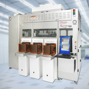
PLAINVIEW, N.Y., Feb. 28, 2019—Veeco Instruments Inc. (NASDAQ: VECO) today announced that SkyWater Technology Foundry has taken delivery of the WaferStorm® single wafer wet process system to support advanced development work for the design and fabrication of next-generation 3D monolithic System-on-a-Chip (3DSoC) technology. One of the most advanced U.S.-based semiconductor technology foundries, SkyWater is leveraging the process performance and production capabilities of the WaferStorm to create densely integrated logic and memory products. Using breakthrough 3DSoC technology, the foundry is collaborating with researchers at the Massachusetts Institute of Technology (MIT) to set a new threshold for device performance and energy efficiency.

 
“Our selection of the WaferStorm system was based on Veeco’s track record of delivering best-in-class technology for wet processing that enables many leading-edge applications,” stated Thomas Sonderman, president of SkyWater. “The solvent-based platform offers a precise level of control during wafer processing, which is essential to the innovations we are working on with MIT to develop technology that drives better performing devices at lower cost.”

WaferStorm’s unique ImmJET™ solvent technology provides customers with the best overall process performance, flexibility and production capability in its class compared to conventional batch or spray-only approaches. WaferStorm offers proven, reliable solutions for metal lift-off (MLO), photoresist strip, dry film resist strip, via cleans, flux removal and other advanced packaging processes. WaferStorm is also the production tool of record for MLO at several leading vertical-cavity surface-emitting laser (VCSEL) manufacturers today.

“SkyWater’s selection of the WaferStorm further showcases Veeco’s leadership in advanced wet processing technology, and we’re pleased to be working with the renowned foundry that is driving true innovation in the 3DSoC space,” said Scott Kroeger, general manager of Veeco’s Precision Surface Processing business unit. “Our full suite of solvent, clean and etch technologies is ideally suited to help create a new class of microelectronic devices and systems that extends beyond previous thresholds for performance and efficiency.” As reported by IEEE, advances in monolithic 3D integration lay the foundation for highly efficient next-generation computing systems. With the emergence of artificial intelligence, edge computing and deep learning driving innovation in memory access as a key enabler for future systems design, the use of 3DSoC represents a paradigm shift for the computer industry and high-tech world. As the industry reaches the next-generation of 3DSoC technology, WaferStorm delivers excellent process results at the lowest cost of ownership, enabling innovators like SkyWater and MIT to advance research and enhance device performance.

Matheson Acquires HyCO Business from Linde


MATHESON, a wholly owned subsidiary of TNSC Group, has completed its acquisition of the divested Linde HyCO business in the United States that became available as a result of the global business combination of Linde and Praxair. The United States Federal Trade Commission approved MATHESON as the buyer of the divested HyCO business on February 27, 2019.

HyCO is an industry term covering the production of hydrogen, carbon monoxide, or syngas, which is a mixture of hydrogen, carbon monoxide and carbon dioxide.
 
Source : 4-traders LINK