Umicore reports: Umicore’s business unit Precious Metals Chemistry inaugurated today its innovative production unit for advanced metal organic precursor technologies used in the semiconductor and LED markets, respectively TMGa (Trimethylgallium) and TEGa (Triethylgallium). The event was attended by European and overseas customers as well as local and regional politicians. The guest of honour was Dr. Barbara Hendricks, Germanys Federal Minister for the Environment, Nature Conservation, Building and Nuclear Safety.
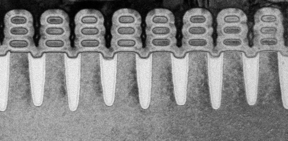
Umicore TMGa (Trimethylgallium) and TEGa (Triethylgallium) facility in Hanau, Germany (photos supplied by Umicore).
Umicore’s TMGa manufacturing process is innovative and unique. It offers a more sustainable and ecological production method by minimizing hazardous side streams and material losses and optimizing yield to nearly 100%. This makes it superior to all existing manufacturing methods in the industry.
Umicore TMGa (Trimethylgallium) and TEGa (Triethylgallium) facility in Hanau, Germany (photos supplied by Umicore).
Dr Lothar Mussmann, Vice-President of Umicore Precious Metals Chemistry said “I am proud that this patented innovation has now become a world-class and industrial scale manufacturing plant. It will provide benefits for our customers and the environment and underlines Umicore’s position as a pioneer in sustainable technologies.”
Umicore TMGa (Trimethylgallium) and TEGa (Triethylgallium) facility in Hanau, Germany (photos supplied by Umicore).
Umicore Precious Metals Chemistry is the only European manufacturer of TMGa and TEGa and supplies customers across the world from its Hanau manufacturing base. Umicore Precious Metals Chemistry helps to reduce cost of ownership through its innovative approach to process chemistry and its collaborative approach with customers and end users.


