Monday, January 29, 2018

Apple chip maker TSMC plans 5-nanometer chips for 2020, 3-nanometer in 2022


Apple’s chip manufacturer TSMC today broke ground on its first 5-nanometer fabrication facility in Taiwan, promising that 5-nanometer chips will be commercially available in 2020, with 3-nanometer chips planned for 2022. The tiny new processors will guarantee that future smartphones continue to shrink while offering superior performance and battery life to today’s models.

First shown in physical form by IBM and Samsung last June, the 5-nanometer chip process is capable of squeezing 30 billion transistors — digital on-off switches — into fingernail-sized chips, doubling or tripling the transistor counts of 10-nanometer chips. TSMC’s 5-nanometer process uses extreme ultraviolet lithography, requiring an expensive super-fine laser that has only recently become commercially viable.


Source: VentureBeat LINK

EXALOS orders Veeco's Propel GaN MOCVD platform for R&D on SLEDs


Epitaxial deposition and process equipment maker Veeco Instruments Inc of Plainview, NY, USA says that EXALOS AG of Schlieren, Switzerland has ordered a Propel gallium nitride (GaN) metal-organic chemical vapor deposition (MOCVD) system (for delivery in third-quarter 2018) for R&D on broadband superluminescent light-emitting diodes (SLEDs).

As a hybrid between LEDs (which emit broadband light from a surface in all directions) and laser diodes (which emit narrowband light from a waveguide with a well-defined laser beam), superluminescent LEDs emit broadband light in a highly directional beam through electrical current injection, and are used in medical and industrial imaging, motion control detectors, navigation, optical sensing and metrology applications.


Source: Semiconductor Today LINK

Friday, January 26, 2018

Sino IP Office Rules in Favor of AMEC by Rendering Veeco Instruments' Susceptorless Reactor Patent Invalid

AMEC
SHANGHAI, Jan. 26, 2018 /PRNewswire/ -- Advanced Micro-Fabrication Equipment Inc. (AMEC) today announced that the Patent Re-examination Board (PRB) of the State Intellectual Property Office (SIPO) in China, ruled on Jan. 23 that all patent claims relating to patent number ZL 01822507.1 held by Veeco Instruments Inc. (Veeco U.S.), and titled "Susceptorless reactor for growing epitaxial layers on wafers by chemical vapor deposition", are invalid. The court cited "lack of novelty and non-obviousness" for its decision.

The patent ruled invalid is the Chinese counterpart of the patents (U.S. 6506252 and U.S. 6726769) asserted by Veeco U.S. in an infringement action taken last year against AMEC's wafer carrier supplier, and filed in the U.S. District Court for the Eastern District of New York.

TSMC Orders Equipment Worth T$2.7 Bln From Tokyo Electron & Applied Materials

Jan 24 (Reuters) - Taiwan Semiconductor Manufacturing Co Ltd :  BRIEF-TSMC Orders Equipment Worth T$2.7 Bln From Tokyo Electron, Applied Materials South East Asia

Source: Reuters

Read full article >

TSMC To Create First 5nm & 3nm SoCs In 2019/2020

According to recent reports cited by Taiwanese media outlets, chipmaker TSMC is planning to start producing of its first 5nm chipsets in 2019, and by 2020 the company intends on manufacturing its first 3nm solution. By the end of the month the tech giant will reportedly start building a new factory in the Southern Taiwan [...]The post Report: TSMC To Create First 5nm & 3nm SoCs In 2019/2020 appeared first on AndroidHeadlines.com |.

Source: AndroidHeadlines

Read full article

TSMC 

Chip maker SK Hynix's 4Q net profit doubles to record high

SEOUL, South Korea (AP) — SK Hynix said Thursday its fourth quarter net profit doubled from a year earlier to a record high and forecast that robust demand for chips would continue this year.
South Korea’s second-largest chipmaker said its October-December earnings jumped to 3.2 trillion won ($3 billion) from 1.6 trillion won a year earlier. Its quarterly sales and operating profit were also at the highest levels in the company’s history. Quarterly sales surged 69 percent to 9 trillion won ($8.5 billion) while operating profit more than doubled to 4.5 trillion won ($4.2 billion).

Read full article


Saturday, January 20, 2018

Alkane - Hafnium product breakthrough consolidates Dubbo Project business case

Alkane - Hafnium product breakthrough consolidates Dubbo Project business case.

Summary
  • Alkane’s wholly owned subsidiary, Australian Strategic Materials Ltd (ASM), has developed high‐purity hafnium dioxide products tailored to meet market requirements.
  • Hafnium oxide exceeding 99.8% HfO2, and 99.9% (Hf+Zr)O2, has been produced using a proprietary process to separate hafnium from zirconium at the demonstration pilot plant at ANSTO.
  • Over the past 12 months, ASM has consulted extensively with industry to confirm growing market demand for high‐purity hafnium, which currently depends on supply from the production of zirconium metal for specialty alloys and the nuclear industry.
  • Global shortage of hafnium anticipated as demand is poised to outstrip current supply.
  • Hafnium metal for super alloys is currently trading in a US$800 ‐ $900/kg range. The ASM business case assumes a conservative product price of US$500/kg for its oxide.
  • ASM will initially produce 25tpa hafnium to meet projected market demand, ramping up to higher quantities as required.

Download : Download (PDF, 718KB)

Development of high‐purity hafnium dioxide

Australian Strategic Materials Ltd (ASM), a wholly owned subsidiary of Alkane Resources, has successfully developed a high‐purity hafnium dioxide (HfO2) product that will be directly marketable as a feed material for a number of downstream applications and for producing metallic hafnium. The technical specifications of this material have been tailored to meet global market requirements, following extensive industry consultation over the past 12 months. 

Monday, January 15, 2018

Picosun to provide 300 mm ALD cluster tool for STMicroelectronics Power Semiconductors

ESPOO, Finland, 16th January, 2018 – Picosun Oy, a leading supplier of Atomic Layer Deposition (ALD) thin film coating technology for global industries, partners with STMicroelectronics S.r.l. to develop the next generation 300 mm production solutions for advanced power electronics.

Power electronic components are right at the heart of many core elements of our society, where energy saving, sparing use of natural resources, and CO2 emission reductions are called for to provide for sustainable future. Energy production with renewables such as wind and solar, clean transportation with electric vehicles and trains, and industrial manufacturing with energy-smart power management and factory automation are key markets where the demand for advanced power components is increasing.


Most power semiconductor industries use 200 mm wafers as substrates. Transfer to 300 mm enables more efficient, ecological, and economical production through larger throughputs with relatively smaller material losses, and adaptation of novel manufacturing processes such as ALD allows smaller chip sizes with increased level of integration.

As a part of the funded project R3-POWERUP (*), Picosun’s PICOPLATFORM™ 300 ALD cluster tool will be optimized and validated for 300 mm production of power electronic components. The SEMI S2 certified PICOPLATFORM™ 300 cluster tool consists of two PICOSUN™ P-300S ALD reactors, one dedicated for high-k dielectric oxides and one for nitrides, connected together and operated under constant vacuum with a central vacuum robot substrate handling unit. The ALD reactors are equipped with Picosun’s proprietary Picoflow™ feature which enables conformal ALD depositions in high aspect ratios up to 1:2500 and even beyond. Substrate loading is realized with an EFEM with FOUP ports. The fully automated cluster tool can be integrated into the production line and connected to factory host via SECS/GEM interface.

“Our PICOPLATFORM™ 300 cluster tools have already proven their strength in conventional IC applications, so expansion to the power semiconductors is only natural. We are very pleased to work with a company such as STMicroelectronics to tailor and validate our 300 mm ALD production solutions to this rapidly growing market. This is also a prime opportunity both to contribute to the future of European semiconductor industries, and to utilize ALD to provide technological solutions to the global ecological and societal challenges such as climate change and dwindling natural resources,” summarizes Juhana Kostamo, Managing Director of Picosun.

Saturday, January 13, 2018

MPD Chemicals Acquires Specialty Chemical Manufacturer Norquay Technology

Norqay Technology, a company with more that 30 years experience in organo metallic precursors for ALD and CVD has just been acquired by MPD Chemicals. Please find press release below.

TREVOSE, Pa., Jan. 11, 2018 /PRNewswire/MPD Chemicals (MPD), a US-based manufacturer of specialty chemicals and custom synthesis solutions, announced today the expansion of its manufacturing capabilities, product portfolio and customer base with the acquisition of Norquay Technology, Inc. (Norquay). Located in Chester Pennsylvania, Norquay is the fourth acquisition to be integrated into the MPD Holdings platform, an Addison Capital portfolio company; existing MPD businesses include Monomer Polymer & Dajac Labs, Silar, and IsoSciences.

Norquay is a specialty chemical manufacturer with over 30 years of expertise in providing the scale-up and production of advanced proprietary custom materials, including organometallic, inorganic and organic molecules. Norquay’s product line includes chromic, electronic, catalyst, ligand, medical adhesive and UV performance products, with a customer base that ranges from startups to large multi-national corporations.

Tuesday, January 9, 2018

Osram orders multi-reactor Propel HM and K475i MOCVD systems from Veeco for high-volume photonics and LED applications

Epitaxial deposition and process equipment maker Veeco Instruments Inc of Plainview, NY, USA says that Osram Opto Semiconductors GmbH of Regensburg, Germany has ordered a multi-reactor Propel High-Volume Manufacturing (HVM) gallium nitride (GaN) metal-organic chemical vapor deposition (MOCVD) system, as well as K475i MOCVD systems. 

The K475i system incorporates Veeco’s Uniform FlowFlange technology, producing films with very high uniformity and improved within-wafer and wafer-to-wafer repeatability with what is claimed to be the industry’s lowest particle generation for demanding applications like photonics and advanced LEDs.  

Source: Semiconductor Today LINK

Saturday, January 6, 2018

Fabless IC Company Sales Top $100 Billion for First Time Ever

Fabless IC Company Sales Top $100 Billion for First Time Ever.

Lam Research and Tokyo Electron took market shares in 2017

Currently the fabs are running hot and expanding and 2018 is expected to continue to grow according to OEMs and market research companies like o VLSI Research (CEO Dan Hutcheson, see below). Solid State Technology reports, based on recent market research by The Information Network (LINK) that Market leader Applied Materials lost market shares in 2017 to the main competitor Tokyo Electron and Lam Research.

"Applied Materials 1.3 share points, dropping from 28.2% in 2016 to 26.9% YTD (year to date). Gaining share are Tokyo Electron Ltd. (TEL), which gained 2.4 share points while rising from 17.0% in 2016 to 19.4% in 2017 YTD. Lam Research gained 1.6 share points and growing from a 19.0% share in 2016 to a 20.6% share in 2017 YTD."

The three companies compete in the following areas with huge growth due to the memory boom in 2017 (3DNAND and DRAM):

  • conductor and dielectric etch equipment
  • deposition equipment - single/multiwafer ALD and CVD
CVD equipment share is roughly 3X that of ALD and ALD passed PVD in 2015 (according to VLSI Research). Furnace ALD and CVD is dominated by Tokyo Electron and Kokusai, however it is a smaller segment as compared to single and multi wafer ALD and CVD. ASMI, the leader in ALD single wafer equipment does not seem to have been able to grow with memory, down from 2.0% to 1.7%.

Please find the full article here: LINK


Friday, January 5, 2018

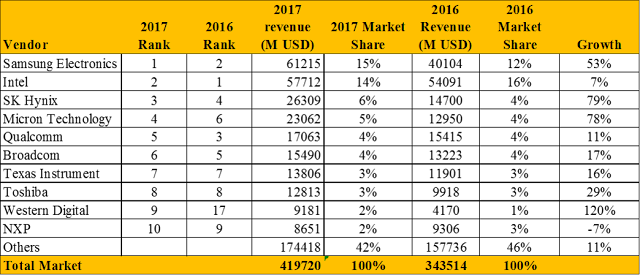
Memory chips led the way in 2017 boosting a 22% record semiconductor growth in revenue

Memory chips (DRAM & FLASH) led the way in 2017 boosting a 22% record semiconductor growth in revenue. Samsung Electronics became the number 1 in overall semiconductor sales for the first time, displacing Intel, which had held the top spot in sales every year since 1992. 


EE Times reports : Semiconductor sales grew by 22 percent to reach a record $419.7 billion — with memory chips leading the way — according to a preliminary estimate by market research firm Gartner.

Gartner (Stamford, Conn.) estimates that increased sales of memory chips due to shortages of NAND flash and DRAM accounted for about two-thirds of overall chip market growth in 2017. Memory also become the single largest semiconductor products category last year, according to the firm.

Full story: LINK


Gartener 2016 to 2017 revenue change for Top 10 Semiconductor companies [replotted]

Tuesday, January 2, 2018

Get back to work - SEMI projects continued boom in fab equipment spending for 2018

MILPITAS, Calif. ─ January 2, 2018 ─ The year-end update to the SEMI World Fab Forecast report reveals 2017 spending on fab equipment investments will reach an all-time high of $57 billion. High chip demand, strong pricing for memory, and fierce competition are driving the high-level of fab investments, with many companies investing at previously unseen levels for new fab construction and fab equipment. See figure 1.
World Fab Forecast Figure 1
Figure 1


The SEMI World Fab Forecast data shows fab equipment spending in 2017 totaling US$57 billion, an increase of 41 percent year-over-year (YoY). In 2018, spending is expected to increase 11 percent to US$63 billion.

While many companies, including Intel, Micron, Toshiba (and Western Digital), and GLOBALFOUNDRIES increased fab investments for 2017 and 2018, the strong increase reflects spending by just two companies and primarily one region.

ALD NanoSolutions Prepares particle coating CVR for Factory Installation

Here is some ALD news for Boulder Colorado just before the Holiday Season (teaken from their excellent e-mail News letter) - Merry Christmas and Happy New Year to the ALD experts in Boulder and elsewhere! 

  • ALD NanoSolutions Prepares CVR for Factory Installation
  • ALD Nano’s Coated Materials were on the International Space StationInternational
  • Organization for Standardization (ISO) Compliance for ALD-Coated Commercial Powders 
As reported in a previous edition of the ALD NanoSolutions Enews (see ALD Nano Enews: Vol. 2, Issue 3), the company announced commercial-scale validation of its continuous ALD reactor system equipment for particles. 

ALD NanoSolutions Prepares CVR for Factory Installation

As reported in a previous edition of the ALD NanoSolutions Enews (see ALD Nano Enews: Vol. 2, Issue 3), the company announced commercial-scale validation of its continuous ALD reactor system equipment for particles. The key aspects of that article are in italics below:

The scientific, process development and engineering teams at ALD Nano have spent considerable resources over the past few years rapidly developing this first-of-its-kind technology from research scale, bench-top to the current commercial-scale systems. A continuous vibrating reactor, or CVR, provides ALD coating capacity of more than three tons per day and 1,200 tons per year of particle materials. These techniques gained from equipment development open up new pathways for ALD Nano's growth. The CVR is a spatial ALD reactor system and can also be utilized for MLD techniques, run at atmospheric or pressurized conditions, and fitted with various features such as plasma.

The company is scheduled to install the first of its CVR reactor systems, second-generation design, in a commercial advanced materials coating production facility in the US in Q1 2018. An important milestone to compliment this type of state-of-the-art progress at the ALD Nano facility in Broomfield, Colorado. Additional CVR reactor systems are to be installed in other commercial materials production facilities over the next few years. Let us know if you have an ALD coating need for advanced materials that requires this level of scale.

Aveni extends copper interconnects to 5nm and below for BEOL integration employing ALD TaN & CVD Co barrier/seed

Recently at IEDM 2017 IBM announced that copper is here to stay and can continue to be scaled for the future back end of line (BEOL) interconnects - 20 Years of Cu BEOL in Manufacturing, and its Future Prospects (Invited), D. Edelstein, IBM TJ Watson Research Center (LINK)

Before the actual copper plating process, the advanced dual-damascene structures for interconnects employ two very important conformal deposition processes :
  • an atomic layer deposition tantalum nitride (ALD TaN) copper diffusion barrier
  • a thin chemical vapor deposition cobalt (CVD Co) liner
More detailed information on Cobalt CVD for barrier/seed and selective encapsulation of copper from the leader Applied Materials can be found here (LINK).

According to a press release below (LINK), Aveni has announced it has obtained results that support the continued use of copper in the BEOL for advanced interconnects, at and beyond the 5nm technology node. Aveni is a French developer and manufacturer of wet deposition technologies and chemistries for 2D interconnects and 3D through silicon via packaging. The company was originally founded in 2001 as a spinoff from the Commissariat à l’énergie atomique et aux énergies alternatives (CEA) to develop and market groundbreaking nanometric deposition technologies for a variety of electronic applications.  

MASSY, France – Dec. 12, 2017 – aveni S.A., developer and manufacturer of market-disrupting wet deposition technologies and chemistries for 2D interconnects and 3D through silicon via packaging, today announced it has obtained results that strongly support the continued use of copper in the back end of line (BEOL) for advanced interconnects, at and beyond the 5nm technology node.

HHV launch ALD System based on technology transferred from IIT Bombay

Hind High Vacuum Co. Pvt. Ltd. (HHV), a vacuum science and technology company with major clients like HAL, ISRO, BARC, Titan etc, announced the launch of its first indigenously developed Atomic Layer Deposition (ALD) System based on technology transferred from IIT Bombay. This tool was developed entirely by HHV’s Thin Film Technology Division out of its Bengaluru facility as a part of the company’s on-going ‘Make in India’ initiative.


A picture of the ALD 150 system, which seems to be a top loaded tool very similar in layout to e.g. a CNT Savannah. Judging by the name this is a 150 mm system (picture from HHV webpage)

Full story: HHV develops Atomic Layer Deposition System based on technology transferred from IIT Bombay

Press release: LINK

Link to HHV ALD product page: LINK

General Motors and Forge Nano has co-developed ALD technology for lithium batteries

According to recent news releases General Motors and Forge Nano has co-developed and been rewarded for ALD for lithium battery technology featuring:
  • ultrathin (thickness < 5nm) multifunctional hybrid coatings and processes.
  • solutions to critical issues involved with gas generation, manganese dissolution induced capacity loss and safety issue associated with polymeric separators.
  • scale-up production and commercialization of this innovation for both automotive and non-automotive applications.
  • semi-continuous ALD systems (the tall pilot-scale stack, as well as the large single-cycle stack), have the production capacity of more than 1 MT/day, making it possible to implement the advanced surface coating technologies into the next generation of lithium ion batteries.
 
Background information:

LOUISVILLE, CO - Forge Nano, Louisville, Colorado, recently won a 2017 R&D 100 Award as co-developer with General Motors for the development of the Ultrathin Multifunctional Hybrid Coatings and Processes. The R&D 100 Awards have served as an innovation awards program for the past 55 years, honoring great R&D pioneers and their revolutionary ideas in science and technology.

“Forge Nano was founded with a vision to deploy precision nano-coatings to make many other technologies safer, less expensive and more efficient. That vision is now a reality, and it is extremely gratifying to be honored by the R&D 100 Awards for introducing one of 2017’s most innovative and influential technology solutions,” said Forge Nano Founder and CEO Dr. Paul Lichty, who accepted the award at the R&D 100 Conference in Orlando, Florida.

Forge Nano launched in 2013 with breakthrough technology that makes nano-coatings fast, affordable and scalable in manufacturing. The company specializes in nano-coatings and atomic film deposition, serving functions from corrosion resistance to electrical insulation or conduction. As demands for next-generation materials become more and more extreme, nano-engineered surface coatings can fulfill the need for enhanced properties and precise characteristics.


The R&D 100 Award - Ultrathin multifunctional hybrid coatings and processes (LINK)

The majority of battery failure initiates from active material surfaces in the electrodes. Surface coatings, as an effective mitigating strategy, have been widely applied into battery material manufacturing process to protect active materials. Conventional coating technologies, such as chemical vapor deposition, physical vapor deposition and wet chemistry, typically generate non-uniform coating particularly on nano-sized particles. The thickness control becomes difficult, and the thicker coating typically induce high much impedance. To tackle this challenge, General Motors—a pioneer in applying surface coating using the Atomic Layer Deposition (ALD) technique—has developed several Ultrathin multifunctional hybrid coatings and processes. These ultrathin (thickness < 5nm) multifunctional coatings solve critical issues involved with gas generation, manganese dissolution induced capacity loss and safety issue associated with polymeric separators. Forge Nano has developed the technologies that enable scale-up production and commercialization of this innovation for both automotive and non-automotive applications. Their semi-continuous ALD systems (the tall pilot-scale stack, as well as the large single-cycle stack), have the production capacity of more than 1 MT/day, making it possible to implement the advanced surface coating technologies into the next generation of lithium ion batteries.