IBM
together with Samsung and Globalfoundries shows off the world´s first 5
nm logic chip with horizontal Gate All Around Field Effect Transistors
also referred to as GAAFETs. GAAFETs are a evolutionary development out
of FInFETS that were fisrt introduced at 22 nm by Intel. It is predicted
that 7nm will be the last FinFET node and that GAAFETs has to be
introduced by then.
Source: IBM LINK
Source: IBM LINK
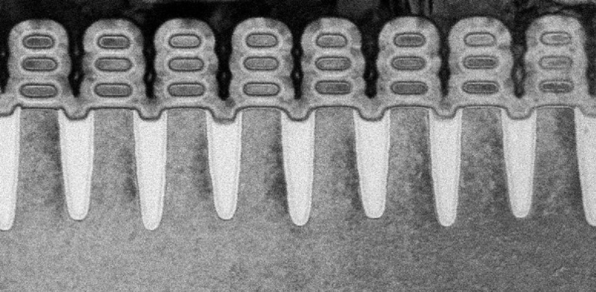
TEM cross section of 5nm GAAFETs by IBM, Samsung and Globalfoundries (Source IBM)
The GAAFETs are manufactued by deposition stacks of epitaxial silicon and silicon germanium
(Si/SiGe Epi). Then by using a combination of EUV lithography and reportedly (LINK)
Atomic Layer Etching (ALE) trenches are etched to separate the stack
into fins and then afterwards to individual nanowires (or nano sheets as
IBM calls them) of Si resp SiGe forming the channels stacked on top of
each other. Later the high-k / metal gate (HKMG) stack is deposited in
by a sequence of ALD processes conformally covering the nanowire
channels.
In the nano sheet FETs, the wires are much wider and thicker presumably giving the nano sheet FETs better electrostatics and drive current
In the nano sheet FETs, the wires are much wider and thicker presumably giving the nano sheet FETs better electrostatics and drive current
Articles :
Want a smarter phone? IBM and Samsung bring you: Nanosheets!
CNET
If you're frustrated with smartwatches that aren't that smart or phones that don't pack enough power, IBM and Samsung have some good news ...
CNET
If you're frustrated with smartwatches that aren't that smart or phones that don't pack enough power, IBM and Samsung have some good news ...
No comments:
Post a Comment