Friday, August 31, 2018

Announcing Kronos™ 1080 and ICOS™ F160 Inspection Systems: Expanding KLA-Tencor's IC Packaging Portfolio

KLA-Tencor has announced it is expanding its integrated circuit (IC) packaging portfolio with two new defect inspection products designed to address a wide variety of IC packaging challenges: KronosTM 1080 and ICOS™ F160. The two new inspection systems join KLA-Tencor’s portfolio of defect inspection, metrology and data analysis systems that help accelerate packaging yield and increase die sort accuracy. You may find the official release here;

Highlights: 
  • Kronos 1080 – offers production-worthy, high sensitivity wafer inspection for advanced packaging, providing key information for process control and material disposition.
  • ICOS F160 – examines packages after wafers have been diced, delivering fast, accurate die sort based on detection of key defect types—including sidewall cracks, a new defect type affecting the yield of high-end packages. 
 Kronos™ 1080 and ICOS™ F160 (Image shared by KLA-Tencor)

Aixtron: HLJ Technology Adds MOCVD Technology from AIXTRON

New customer will use AIX 2800G4-TM system to increase manufacturing capacity and epitaxial wafer size. AAIXTRON SE announced that HLJ Technology Co., Ltd., a Taiwanese VCSEL epitaxy and chip manufacturer, has ordered multiple AIX 2800G4-TM MOCVD sets to increase its wafer capacity as well as its epitaxial wafer size production line from 4-inch to 6-inch for high-volume manufacturing of vertical-cavity surface emitting lasers (VCSEL). AIXTRON’s fully automated Planetary Reactor systems will be supplied in 8x6-inch configuration in the course of Q4/2018 and beyond.

Source: LINK


Wednesday, August 29, 2018

Micron to invest $3 billion in memory chip factory in Manassas, Virginia

[Venture Beat] Manassas, Virginia is best known as the site of the Battle of Bull Run in the American Civil War. And now it's home to an expanding chip factory, as Micron Technology announced today it is investing $3 billion by 2030 to make memory chips. 
 
Picture credit Micron.com
 
Boise, Idaho-based Micron makes dynamic random access memory (DRAM), the chips that provide the memory for applications in personal computers and many other devices. It will also make NAND flash memory chips for long-term storage in a wide variety of devices.

The investment breaks down to about $250 million per year over 12 years, and it will create about 1,100 new jobs. That’s not a huge amount, but it does represent a commitment to keeping manufacturing and high-wage jobs in the U.S. at a time when the rest of the world is increasingly competitive at making chips, or the basic building blocks of electronic devices. 
 
Source: Venture Beat [LINK]

Monday, August 27, 2018

GLOBALFOUNDRIES Reshapes Technology Portfolio to Intensify Focus on Growing Demand for Differentiated Offerings

Santa Clara, Calif., August 27, 2018 – GLOBALFOUNDRIES today announced an important step in its transformation, continuing the trajectory launched with the appointment of Tom Caulfield as CEO earlier this year. In line with the strategic direction Caulfield has articulated, GF is reshaping its technology portfolio to intensify its focus on delivering truly differentiated offerings for clients in high-growth markets.

GF is realigning its leading-edge FinFET roadmap to serve the next wave of clients that will adopt the technology in the coming years. The company will shift development resources to make its 14/12nm FinFET platform more relevant to these clients, delivering a range of innovative IP and features including RF, embedded memory, low power and more. To support this transition, GF is putting its 7nm FinFET program on hold indefinitely and restructuring its research and development teams to support its enhanced portfolio initiatives. This will require a workforce reduction, however a significant number of top technologists will be redeployed on 14/12nm FinFET derivatives and other differentiated offerings.
Globalfoundries Fab 8 Malta, NY (picture credit Globalfoundries.com).
“Demand for semiconductors has never been higher, and clients are asking us to play an ever-increasing role in enabling tomorrow’s technology innovations,” Caulfield said. “The vast majority of today’s fabless customers are looking to get more value out of each technology generation to leverage the substantial investments required to design into each technology node. Essentially, these nodes are transitioning to design platforms serving multiple waves of applications, giving each node greater longevity. This industry dynamic has resulted in fewer fabless clients designing into the outer limits of Moore’s Law. We are shifting our resources and focus by doubling down on our investments in differentiated technologies across our entire portfolio that are most relevant to our clients in growing market segments.”

Saturday, August 18, 2018

BOE to begin trial production of micro-OLED in early 2019 using ALD

[DigiTimes LINK] BOE Technology is making preparations for trial production of micro-OLED panels for AR/VR applications, according to a Korea-based ET News report. The report claims the follwoing:
  • production is planned for Kunming BOE Display Technology - a joint venture between BOE and the provincial government of Kunming in China.
  • BOE has begun purchasing production equipment needed for the plant, including sputters, CVD (chemical vapor deposition), AOI (automated optical inspection) and ALD (atomic layer deposition) equipment, to pave the way for the trial production set in early 2019.
  • Kunming BOE Display aims to roll out one millions units of OLED panels a year with panel sizes ranging from 0.5- to 0.8-inch. 


BOE Technology detailed a USD170 Million investment in China’s First Micro-OLED Plant in Kunming in 2017 [LINK]. According to the news release Chinese OLED tech firm Olightek Opto-Electronic Technology Co. will invest CNY200 million through OLED micro-display related intangible assets and Dianzhong Industry Development Group Co. will put up CNY95 million. Kopin Technology Shenzhen Co., the Chinese subsidiary of major American electronics manufacturer, Kopin Corp., will provide the remaining CNY35 million.

Kopin has entered the OLED microdisplay market for mobile VR and AR with new technology and business model as a fully Fabless company using foundries for manufacturing. Please check here for a review [LINK]


Tuesday, August 14, 2018

Is the semiconductor industry preparing for ruthenium again?


As cobalt is being implemented for 10/7 nm logic interconnects, the next contender on roadmaps for the leading IDMs and foundries is ruthenium. This is not the first time that ruthenium comes into play, ruthenium has on regular basis been on the DRAM and Logic manufacturers roadmaps. Last year there was several indications that ruthenium is back again including that you could spot a rice in ruthenium metal pricing. However, since I started in the semiconductor world 2003 I think that I have managed to been part of six ALD/CVD ruthenium programs and I am happy that one of them is still running (this was my shortest participation, all in all 7 days).

So why do you want to use an expensive and rather fancy metal like ruthenium in interconnects? The lowest Ru resistivity reported for use in interconnects is 15 μΩ-cm, at a cross-sectional area of 300 nm2. Ru damascene metallization is extendible to features with critical dimension around 10 nm and Ru may match Cu line resistance for line dimensions below ~17 nm.

Therefore, as semiconductor devices become even smaller at sub 7 nm nodes, Ru is a strong candidate for replacing some of the back end and middle of the line Cu as the interconnect material or as a liner/barrier/seed for metallization.

At AVS ALD 2018 in Incheon South Korea there was a high number of presentations on ruthenium. Besides the oral presentations here below there were also a number of interesting posters. You can get the abstracts by searching "ruthenium" in the AVS ALD conference planer (LINK).

Low Temperature Atomic Layer Deposition of Ru for Copper Metallization [Oral]
Anil Mane‚ Yan Zhang (Argonne National Laboratory); Amit Kumar‚ John Allgair (BRIDG); John Hryn‚ Jeffrey W. Elam (Argonne National Laboratory)

Insight in Surface Dependence and Diffusion-mediated Nucleation Mechanism of Ruthenium Atomic Layer Deposition on Dielectrics
Job Soethoudt (KU Leuven‚ Belgium); Yoann Tomczak (IMEC‚ Belgium); Fabio Grillo‚ Ruud Van Ommen (Delft University of Technology‚ Netherlands); Efrain Altamirano Sanchez (IMEC‚ Belgium); Annelies Delabie (KU Leuven‚ Belgium)

Inherent Substrate Selectivity and Nucleation Enhancement during Ru ALD using the RuO4-Precursor and H2-gas.
Matthias Minjauw‚ Hannes Rijckaert‚ Isabel Van Driessche‚ Christophe Detavernier‚ Jolien Dendooven (Ghent University‚ Belgium)
 
Conformal Growth of Low-resistivity Ru by Oxygen-free Thermal Atomic Layer Deposition [Oral]

Guo Liu‚ Jacob Woodruff‚ Daniel Moser (EMD Performance Materials)

Ruthenium: Advanced Nodes and Supply Chain Implications [Oral]
Oliver Briel‚ Don Zeng‚ Andreas Wilk (Umicore AG & Co. KG‚ Germany)
 
The last contribution by Umicore is especially interesting since it explain in great details the whole supply chain of ruthenium today including:
  • Ruthenium in electronic applications
  • Todays Ruthenium market - Platinum Group Metals market
  • Market drivers, Sources, uses, supply vs. demand,
  • Managing Ruthenium in your precursor portfolio
  • Sourcing strategies

Umicore Tweet: Oliver Briel's fascinating talk on ‘: Advanced Nodes and Supply Chain Implications’ (LINK).

Another event taking place this summer was the Imec US Technology Forum in San Fransisco, also here ruthenium was again on the agenda. According to a recent article in C&EA (LINK), reporting from the annual Imec Technology Forum, Imec experts made the case that the metal ruthenium has potential to replace copper in interconnect. Such a replacement could prevent the semiconductor industry from tripping over a wiring problem in coming years. The main information was given in a talk by Zsolt Tokei - Program Director Nano-interconnect, imec:


New Conductors - Reality or not? [LINK]
For several decades Cu, Al and W were used for interconnect wiring. Recently, due to resistance and reliability concerns alternatives to conventional conductors gained significant interest. Alternative metals are of interest to both memory and logic chips. In this talk imec’s conductor research activities will be showcased with a few implementation examples using damascene or subtractive processes. Benchmark to conventional conductors as well as future perspectives will be provided.

Before that there was also the IITC 2018 and there ruthenium was on the agenda as well. One interesting presentation was the Adelman et. al also from Imec, “Alternative Metals: from ab initio Screening to Calibrated Narrow Line Models” (LINK).
So as for now, ruthenium is on the roadmaps for 5 nm and below but not yet implemented in HVM by any Foundry. However there is a reverse engineering report claiming that ruthenium has been found in Intels 10 nm technology [LINK].


Further reading : Ruthenium Liners Give Way To Ruthenium Lines (LINK)

Much more detailed information on ALD/CVD metal precursors : TECHCET LLC Critical Materials Report(TM) on Metal & High-k  CVD and ALD precursors (LINK)


Meaglow Introduces its Hollow Cathode Plasma Sources to Four New Countries

While ALD2018 was going on in Incheon, South Korea, the first Meaglow hollow cathode plasma source in South Korea was being installed at Hanyang University in Ansan.

This is one of a number of firsts for Meaglow this year, we’ve also had our first sale to Israel (to Ben-Gurion University of the Negev), our first sale to Gerrmany (to Otto-von-Guericke University, Magdeburg) and our first sale to the United Kingdom (to the University of Liverpool). All of these sales have been for Meaglow’s popular Series 50 Plasma Source, which is used by many of our customers to upgrade from ICP to hollow cathode plasma operation.

Contact us at info@meaglow.com to learn more about the benefits of Meaglow’s plasma technology.


ALD/CVD Precursors Market Reaches $1.3B by 2023

SAN DIEGO, July 6, 2018 /PRNewswire-iReach/ -- TECHCET—the advisory services firm providing electronic materials information— announced that strong growth in IC fabrication demand for atomic-layer deposition (ALD), chemical-vapor deposition (CVD), and spin-on dielectric (SOD) precursors should result in a combined global market size of US$1.3 billion by the year 2023. Specifically, metal precursors are expected to see a compound annual growth rate (CAGR) of 6.2 percent through 2023 starting from $460 million in revenues for this year, as detailed in the latest TECHCET Critical Materials Report (CMR). The market for dielectric materials is forecasted to be $465 million this year with CAGR of 8.2 percent through 2023, as detailed in the latest CMR. 


"Plasma enhanced CVD and ALD processes drive increasing demand for silicon precursors, used in depositing the 32-72 layers of 3D-NAND chips and in self-aligned multiple patterning for advanced logic and memory chips," explained Dr. Jonas Sundqvist, TECHCET senior analyst and author of the report. "We see a need for more advanced ALD/CVD precursor production in China, to support more leading-edge logic and memory fabs ramping production there."

Cobalt (Co) metal is being used to encapsulate copper on-chip multi-level interconnects in the most advanced logic fabs for both foundries and IDMs. Intel is using full cobalt interconnects to replace some of the copper levels in it's newest logic chips. The conservative demand forecast for cobalt metal in the form of ALD/CVD precursors for logic IC fabs is $25 million in 2018, with considerable growth to $70 million by 2023.

Due to the competitive demand for cobalt needed for the lithium batteries used in EVs, and due to conflict issues in the supply-chain, cobalt metal pricing is volatile and reliable forecasting is correspondingly difficult. To anticipate supply:demand imbalances, TECHCET tracks ALD and CVD precursor demands in competing high volume manufacturing (HVM) industries such as flat-panel display, photovoltaics, MEMS, and LED.

Suppliers covered in this report include: Adeka, Air Liquide, Azmax part of Azuma group, BASF, DNF "Dream New Future", Dow Corning, Digital Specialty Chemicals (DSC), DowDuPont, Entegris, Epivalence, FujiFilm, Gelest, H.C. Starck, Kojundo Chemical Laboratory, Merck's EMD Performance Materials, Nanmat Technology, Norquay Technology, Nova-Kem, Nanogen Solutions, Pegasus Chemicals, Praxair, Soulbrain, STREM, TCI Chemicals, Tri Chemical Laboratories, Umicore, UP Chemical, Versum Materials.

Purchase Reports Here: https://techcet.com/product-category/ald-cvd-precursors/

ABOUT TECHCET: TECHCET CA LLC is an advisory service firm focused on process materials supply-chains, electronic materials technology, and materials market analysis for the semiconductor, display, solar/PV, and LED industries. Since 2000, the company has been responsible for producing the SEMATECH Critical Material Reports, covering silicon wafers, semiconductor gases, wet chemicals, CMP consumables, Photoresists, and ALD/CVD Precursors. For additional information about these reports or CMC Fabs membership please contact Diane Scott at info@cmcfabs.org +1-480-332-8336, or go to www.techcet.com or www.cmcfabs.org.

Media Contact: Lita Shon-Roy, TECHCET CA LLC, 1-480-382-8336, info@techcet.com

News distributed by PR Newswire iReach: https://ireach.prnewswire.com

Wednesday, August 8, 2018

ASM launch ALD Pulsar and PEALD Emerald on XP8 multi-chamber platform

New System Integrates Core Pulsar® and EmerALD® Capabilities with Higher Productivity, Enabled by Multi-Chamber 300mm XP8 Platform

SAN FRANCISCO, California - ASM International N.V. (Euronext Amsterdam: ASM) today announced the Synergis®atomic layer deposition (ALD) tool for advanced-node logic and memory high-volume production applications. The latest addition to ASM's industry-leading line of ALD tools, Synergis leverages ASM's core ALD hardware and process technology, optimized over more than a decade in volume manufacturing, to address a wide range of thermal ALD applications.


Demand for ALD solutions is growing, as it enables the use of new materials and designs for advanced chip manufacturing. The new Synergis system is designed to address a number of key ALD equipment challenges, by providing superior thermal control of the reactor environment, delivery of low-vapor-pressure precursors, purge efficiency and reduced preventive-maintenance cycles. As a result, Synergis delivers excellent conformality and film uniformity with high throughput and low per-wafer cost.

Veeco Firebird(TM) - Batch Thermal ALD for High Volume Production

Earlier this year Veeco launched their new platform for Batch ALD for high volume production and now you can find more details on the Veeco product offering pages: LINK

Firebird - Batch ALD for High Volume Production

The Firebird™ system is a fully automated batch production ALD platform delivering superb uniformity with best-in-class throughput at the lowest possible cost-per-wafer. Integrating proven Veeco automation solutions, it enables safe wafer handling via low-impact batch transfer. Its modular pre-heat & cool-down design enables a flexible thermal management solution tailored around your specifications. The Firebird™ system’s high capacity reactor(s), low consumables/maintenance costs and compact footprint deliver the most cost-effective solution while exceeding your throughput requirements.

Firebird™ - ALD System for Specialized Wafer Production 

Key features include:

  • Ideal for oxide films, including encapsulation & barrier layers, optical coating
  • Best-in-class throughput (up to 40,000 wafers per month)
  • Proven Veeco automation
  • Safe wafer handling for fragile / temperature sensitive substrates (e.g., LNO / LTO / glass)
  • Modular thermal management for optimal process flexibility and throughput
  • Worldwide sales, service and support

Configurability advantage

The modular system configuration can be effectively tailored to minimize process flow bottlenecks and offers outstanding processing flexibility.

 2 reactors, 1 heat-up module

1 reactor, 2 heat-up modules

Thursday, August 2, 2018

Beneq present how to minimize circuit board maintenance with ALD

ALD for moisture protection

Wherever we have electronics, we have circuit boards (CB). The ever-increasing demand for higher performance of electronics in more demanding environmental conditions is pushing the limits of current circuit board packaging technologies’ performance. If the circuit boards are designed and assembled well, they should endure in the environment they are intended to work in. However, in new challenging environments, CBs may need maintenance more often than would be desirable. Usually moisture and temperature are the greatest threats to circuit boards and they accelerate failure generation.


Electrochemical migration (ECM) is one nasty phenomenon in circuit assemblies. What it needs to be manifested is moisture, electrical current and conductive residues. When an electronic product is in use, there is obviously current available for the ECM to happen. To effectively prevent ECM, one needs to either eliminate moisture or the residues.

Full article: Beneq Blog (LINK)

Monday, July 30, 2018

Gelest Announced Diiodosilane Commercialization for PEALD Silicon Nitride

MORRISVILLE, Pa., July 27, 2018 — Semiconductor material Gelest Inc. has announced the commercializing of diiodosilane to meet the global demand of the semiconductor industry for next-generation semiconductor chips.

Diidosilane (LINK)

Gelest’s dedicated diiodosilane plant in Morrisville is fully operational and can produce commercial quantities of diiodosilane with purity in excess of 99.9 percent. Diiodosilane is a key chemical precursor used by semiconductor companies worldwide in the development and scale-up of next-generation semiconductor chips that require high-throughput, highly conformal silicon nitride thin films.

Diiodosilane is typically deposited by plasma-enhanced atomic layer deposition to create the silicon nitride thin film. Gelest sees a significant increase in demand for high purity diiodosilane driven by development and production of semiconductor chips requiring silicon nitride thin films at low thermal budgets.

Gelest is a manufacturer of specialty materials for the semiconductor industry.

Source : Photonics LINK

Gelest is sponsoring and exhibiting at the AVS ALD2018 conference currently taking place in South Korea (LINK)  

Wednesday, July 25, 2018

ASM International N.V. 2018 Q2 - Results

ASM International N.V. (Euronext Amsterdam: ASM) today reports its second quarter 2018 operating results (unaudited) in accordance with IFRS. (LINK)
  • New orders received of €176 million.
  • Net sales for the second quarter 2018 were €209 million, an increase of 31% compared to the previous quarter.
  • Gross profit margin was 42.1% in Q2 2018 compared to 37.8% in the previous quarter.
  • Operating result increased to €38 million compared to the previous quarter. The increase is mainly the result of the higher sales level and higher gross margin.
  • Normalized net earnings for the second quarter 2018 increased by €44 million compared to Q1 2018.
Earnings Call slide deck (Seeking Alpha) : LINK
 
 
COMMENT

Commenting on the results, Chuck del Prado, President and Chief Executive Officer of ASM International said:

"In Q2 we realized sales of €209 million and an order intake of €176 million. Both sales and order intake were within our guidance, despite the uncertainty around the exact timing of individual tools as mentioned in the Q1 earnings release. The gross margin in Q2 at 42% returned back again in the range of low to mid 40's. This month at Semicon West, we introduced the Synergis, the latest addition to ASM's industry-leading line of ALD tools, which addresses a wide range of advanced applications and will drive expansion of our Served Available Market within single-wafer ALD."

OUTLOOK

For Q3, on a currency comparable level, we expect sales of €180-200 million and an order intake of € 200-230 million. Q3 reflects still some uncertainty around the exact timing of individual tools.

For 2018, general expectations for growth of the wafer fab equipment market are currently mid to high single digits. Based upon the current market developments we expect our sales in the second half to be stronger than in the first half. We expect to outgrow the wafer fab equipment market in 2018.


Tuesday, July 17, 2018

Changelight orders additional AIXTRON systems

Company expands MOCVD capacity for ROY fine pitch and mini LEDs with AIXTRON's flagship product AIX 2800G4-TM


AIXTRON SE (FSE: AIXA), a worldwide leading provider of deposition equipment to the semiconductor industry, is supplying additional leading-edge MOCVD technology to Xiamen Changelight Co, Ltd (Changelight). Thus, the Chinese company is expanding its production capacities for arsenide-phosphide-based red, orange and yellow LEDs (ROY LED) and solar cells by several AIX 2800G4-TM cluster systems. The tools will be delivered to the customer between Q3/2018 and Q1/2019. 

All production systems have a wafer configuration of 15x4 inches, which enables maximum yield at the highest quality level. Due to its unique production performance and the high manufacturing capacity of AIXTRON's automated Planetary Batch Reactor concept, the AIX 2800G4-TM has established itself as a reference system for the production of ROY LEDs in recent years.

Jin Zhangyu, president of Xiamen Changelight, said: "We have been using AIXTRON's equipment technology to manufacture advanced optoelectronic devices for years and therefore, have great confidence in the AIX 2800G4-TM. The outstanding performance of the system in terms of wafer homogeneity and efficiency in material consumption combined with maximum flexibility and versatility in production will help us to position Changelight as one of the world's leading suppliers of ROY LED for fine pitch, mini LED and micro LED applications."
 
Source: Aixtron (LINK)

Picosun - The ALD Company

While waiting for the ALD2018 in Korea starting you should have a look at the new Picosun promotional video. You can see a number of cool ALD reactors passing by in the background.


Monday, July 9, 2018

Leading memory chip manufacturer purchases multiple VEECO AP300 lithography systems for DRAM interconnect applications

Growing Demand for Advanced Packaging in the Memory Market Highlights Value of Veeco’s
High Volume Manufacturing Lithography Systems


PLAINVIEW, New York, July 9, 2018 – Veeco Instruments Inc. (Nasdaq: VECO) today announced that one of the world’s leading memory chip manufacturers has ordered multiple AP300™ lithography systems to support the fast growing demand for DRAM with copper (Cu) pillars. The company selected the Veeco tools for their versatility in addressing advanced packaging applications, proven reliability in supporting high volume manufacturing and low total cost of ownership. 
This approach echoes a larger industry trend, with more and more memory manufacturers exploring the use of Cu pillars in DRAM interconnect applications due to their higher input/output (I/O) density, improved electrical performance and better thermal efficiency. “Within the DRAM market, the interconnect is shifting from wire bond to flip chip,” said Jan Vardaman, president of semiconductor packaging analyst firm TechSearch International, Inc. “We project that over the next three years, the annual number of flip chip interconnects in DRAM will grow 29 percent on a unit volume basis.”

The AP300 is part of a family of lithography systems built on Veeco’s customizable Unity Platform™, which delivers superior overlay, resolution and side wall profile performance, driving highly automated, cost-effective manufacturing for customers. The system is particularly well suited for Cu pillar, fan-out, through-silicon via (TSV) and silicon interposer applications. A low risk, low cost, high volume manufacturing solution, the AP300 is staged to support rapid market adoption of advanced packaging applications among memory manufacturers.

“The growing demand for innovative, alternative solutions to wire bonding in memory presents a strong opportunity for Veeco,” said Rezwan Lateef, vice president and general manager of lithography products at Veeco. “Furthermore, this significant customer adoption validates the AP300’s ability to address advanced packaging applications in a broader high-volume production market. To meet this demand, we are strengthening our regional technical staff to support numerous memory manufacturers looking to fast-track adoption.”

Veeco will be at Booth #6070 at SEMICON West in San Francisco, CA, July 10-12, 2018.

Sunday, June 17, 2018

Aledia selects Veeco Propel GaN MOCVD platform for large wafer 3D LED production

Veeco Instruments Inc. today announced that Aledia, a developer and manufacturer of next-generation 3D LEDs for display applications based on its gallium-nitride-nanowires-on-silicon platform, has selected Veeco’s Propel® GaN MOCVD system to support advanced research and development. Aledia noted the tool’s large process window, single-wafer reactor technology and defect stability as key factors in its decision to adopt the Propel system.

“We believe that the opportunity for our breakthrough nanowire-LED display technology on large-area silicon is very large, and we need the best and most scalable technology available to support our continued R&D around 3D display applications—we believe Veeco is best positioned,” stated Giorgio Anania, CEO, chairman and co-founder of Aledia. “Veeco’s cutting-edge Propel system delivers unsurpassed results, and very good homogeneity throughout the entire wafer, making it the best choice and one we know will help us continue to push the limits of innovation.”
 
Source:  SolidState Technology (LINK)

Aleida 3D Microwire LED Technology

Aledia is the first company to grow high-density, coaxial gallium nitride (GaN) microwires directly onto large-diameter 200mm silicon wafers (extendable to 300mm wafers) using low-cost processes that are fully compatible with the back end of line of today's semiconductor foundries. When processed these nanowires become LEDs.
 
Aledia's 3D nanowire-on-Silicon LED technology enables the next generation of displays, that can be brighter, can give longer battery life, can have more stable colors, and can be mass manufactured on existing foundries at very competitive cost points. (Aledia.com)
 
 
3D (Microwire) LEDs:
  • Large, economical substrate
  • Fast MOCVD growth process (low capital expenditure)
  • Low materials consumption
  • Existing high-volume silicon wafer fabs
  • Light emission area = up to 3X the 2D area = more light/mm2 or less current density, less efficiency droop
  • Multiple colors on one wafer or even on one chip
 

Thursday, June 14, 2018

Record Equipment Spending Continues in 2018 and 2019

[SEMI] The semiconductor industry is nearing a third consecutive year of record equipment spending with projected growth of 14 percent (YOY) in 2018 and 9 percent in 2019, a mark that would extend the streak to a historic fourth consecutive growth year, according to the latest update of the World Fab Forecast report published by SEMI. The industry last saw four consecutive years of equipment spending growth in the mid 1990s.

  • Korea and China are leading the growth, with Samsung dominating global spending and ascendant China on a fast, steep rise, surging ahead of all other markets.
  • The Europe and Mideastern region will boost investments by 12 percent in 2018, with Intel, GLOBALFOUNDRIES, Infineon and ST Microelectronics as the largest contributors.
  • Japan is beefing up equipment spending by 60 percent in 2018, with the largest increases by Toshiba, Sony, Renesas and Micron.
  • Southeast Asia will increase investments by more than 30 percent in 2018, although total spending is proportionately smaller than in other regions owing to its size. The main contributors are Micron, Infineon and GLOBALFOUNDRIES, though companies including OSRAM and ams are also increasing investments.
  • Americas, i.e., USA grows slightly back to previous level of USD 5 to 6 billion.   
 
Source : SEMI Blog (LINK)
 
 equipment spending by region (includes new and refurbished)

Tuesday, June 12, 2018

Oxford Instruments swings back into profit

Oxford Instruments swung back to a profit in the year to the end of March 2018, driven by a strong performance from its materials and characterisation business and favourable currency movements.
Pre-tax profit came in at £34.2m versus a loss of £26.2m in 2017, although revenue slipped 1.1% to £296.9m.

Meanwhile, reported orders were up 5% to £313m, or 5.8% higher at constant currency, while net debt fell to £19.7m from £109.3m thanks to good operating cash flow and proceeds from the sale of Industrial Analysis.

Adjusted basic earnings per share rose 35.7% to 56.3p and the full-year dividend was lifted 2.3% to 13.3p a share.

The company, which provides high-technology products and systems for industry and research, saw good growth in the early implementation of its Horizon Strategy and a strong financial performance across materials & characterisation, driven by leading product portfolio and customer applications focus in growing markets.

It also saw a good second half performance in research & discovery, which was offset by a weaker first half, while profit and margin growth in the service & healthcare division was driven by services relating to its own products.

Chief executive Ian Barkshire said: "We have made good progress in the year with the early implementation of the Horizon strategy, which was introduced in May 2017.

"We have positioned the group to become a leading provider of high technology products and services to the world's leading industrial companies and scientific research communities to image, analyse and manipulate materials down to the atomic and molecular level. Our chosen end markets remain robust and, combined with our customer applications focus and improved core capabilities, provide strong long-term drivers for future growth and margin improvement."

Saturday, June 9, 2018

TSMC Moving 7nm Chip Process To Mass Production Early

Taiwanese semiconductor giant TSMC has announced that it will be putting its 7nm process into mass production earlier than planned in order to meet demand from clients. Processor makers like MediaTek, Huawei’s HiSilicon, NVIDIA and Qualcomm are all moving into 7nm design and production, and TSMC wants to be able to continue providing them with the silicon they need to get their products up and running. In order to do this, TSMC will speed ahead of the likes of Samsung and Intel, and work to make its 7nm product available to clients as soon as possible.

Source: LINK

Entegris announces agreement to acquire SAES Pure Gas business

Entegris, Inc. (NASDAQ: ENTG), a distributor of specialty chemicals and advanced materials solutions, announced today it has entered into a definitive agreement to acquire the SAES Pure Gas business, from SAES Getters S.p.A. (“SAES Group”), an advanced functional materials company headquartered in Milan, Italy. The SAES Pure Gas business, a provider of high-capacity gas purification systems used in semiconductor manufacturing and adjacent markets is based in San Luis Obispo, California and will report into the Microcontamination Control division of Entegris. Under the agreement, Entegris will purchase the shares and assets which comprise the SAES Pure Gas business for approximately $355 million, subject to customary purchase price adjustments.
 
Source: LINK

Wednesday, June 6, 2018

Applied Materials enables cobalt contact & interconnect for 7nm with pre-clean, PVD, ALD and CVD – on the Endura® platform

At IEDM 2017 in December both Intel and Globalfoundries presented cobalt encapsulation (liner and cap) for copper local interconnects as well as Co fill contacts for their 10nm resp 7nm technologies. Since then many have wondered about the unit process details behind the new cobalt integration and here we have it - The Applied Materials complete cobalt solution as announced yesterday. Especially interesting that TiN ALD also is used as a cobalt seed/adhesio/dufusion barrier for cobalt contacts. The most interesting stuff you will finde here: LINK
[SANTA CLARA, Calif., June 05, 2018]  Applied Materials, Inc. today announced a breakthrough in materials engineering that accelerates chip performance in the big data and AI era.

In the past, classic Moore’s Law scaling of a small number of easy-to-integrate materials simultaneously improved chip performance, power and area/cost (PPAC). Today, materials such as tungsten and copper are no longer scalable beyond the 10nm foundry node because their electrical performance has reached physical limits for transistor contacts and local interconnects. This has created a major bottleneck in achieving the full performance potential of FinFET transistors. Cobalt removes this bottleneck but also requires a change in process system strategy. As the industry scales structures to extreme dimensions, the materials behave differently and must be systematically engineered at the atomic scale, often under vacuum. 
To enable the use of cobalt as a new conducting material in the transistor contact and interconnect, Applied has combined several materials engineering steps – pre-clean, PVD, ALD and CVD – on the Endura® platform. Moreover, Applied has defined an integrated cobalt suite that includes anneal on the Producer® platform, planarization on the Reflexion® LK Prime CMP platform and e-beam inspection on the PROVision™ platform. Customers can use this proven, Integrated Materials Solution to speed time-to-market and increase chip performance at the 7nm foundry node and beyond. 

“Five years ago, Applied anticipated an inflection in the transistor contact and interconnect, and we began developing an alternative materials solution that could take us beyond the 10nm node,” said Dr. Prabu Raja, senior vice president of Applied’s Semiconductor Products Group. “Applied brought together its experts in chemistry, physics, engineering and data science to explore the broad portfolio of Applied’s technologies and create a breakthrough Integrated Materials Solution for the industry. As we enter the big data and AI era, there will be more of these inflections, and we are excited to be having earlier and deeper collaborations with our customers to accelerate their roadmaps and enable devices we never dreamed possible.”

While challenging to integrate, cobalt brings significant benefits to chips and chip making: lower resistance and variability at small dimensions; improved gapfill at very fine dimensions; and improved reliability. Applied’s integrated cobalt suite is now shipping to foundry/logic customers worldwide.

Applied Materials, Inc. (Nasdaq:AMAT) is the leader in materials engineering solutions used to produce virtually every new chip and advanced display in the world. Our expertise in modifying materials at atomic levels and on an industrial scale enables customers to transform possibilities into reality. At Applied Materials, our innovations make possible the technology shaping the future. Learn more at www.appliedmaterials.com.

Sunday, June 3, 2018

The Foundries are aiming at AI chip orders in China with 10/14nm advanced process technologies

[Cage Chao, Taipei; Jessie Shen, DIGITIMES] Semiconductor Manufacturing International (SMIC), and the China-based production subsidiaries of both Globalfoundries and United Microelectronics (UMC) are looking to expand their advanced node offerings for the China market to include 10/14nm as they vie for orders from the local AI chip supply chain, according to industry sources.

Taiwan Semiconductor Manufacturing Company's (TSMC) newly-established Nanjing fab, which has entered directly 16nm FinFET chip production since April 2018, has enjoyed robust orders from China-based AI chip developers eager to accelerate the adoption of advanced process technologies, the sources indicated.

China-based foundries including SMIC, and Globalfoundries' and UMC's production subsidiaries locally have informed their customers they will be capable of providing 10/14nm node manufacturing starting the second half of 2018 or 2019, the sources disclosed.These foundries are looking to catch up with TSMC in China's market for advanced process technologies, the sources said.

Source: Digi Times LINK

Friday, June 1, 2018

Globalfoundries updates on 7 nm and may skip 5 nm

[AnandTech]High-ranking executives of GlobalFoundries this month gave several updates concerning future plans of the contract maker of semiconductors. As it appears, in a bid to provide more tangible advantages to its customers and not to invest in short-lasting nodes, the company is mulling skipping 5 nm manufacturing technology like it did with the 10 nm fabrication process. In addition, the company admits that its only leading-edge fab may not have enough capacity for all of its customers at 7 nm, and some of its clients may need to work with other foundries to meet their demand. 
 
7LP On Track for HVM, But Capacities Are Concern Gary Patton, CTO of GlobalFoundries, said in an interview with EETimes that the company’s first-generation 7LP process technology (7 nm leading performance), which relies exclusively on DUV step and scan systems, is on-track for high-volume manufacturing in the second half of this year. One of the first customers to use this tech will be AMD, which briefly announced its 7LP Vega GPU for a couple of times already. Not everything is rosy with 7LP though.

Full article : LINK

Wednesday, May 30, 2018

ASM International Investor Presentation - Slideshow

The following slide deck was published by ASM International N.V. in conjunction with the Investor Presentation event.
 
Seeking Alpha: LINK
 
ASM International : LINK (pdf)


Friday, May 25, 2018

The blog is down for GDPR alignment

The blog is down for GDPR alignment. Please enjoy the weekend.

TSMC: TSMC is reportedly making 7-nanometer Apple A12 chips for 2018 iPhones

Taiwanese semiconductor manufacturer TSMC has officially started mass-producing 7-nanometer (nm) chips intended for Apple’s 2018 iPhones, Bloomberg reports, setting the stage for annual performance and power efficiency improvements. The new processors are expected to carry Apple’s A12 name this year and to continue at the 7nm size through at least 2019, with the debut of the A13 next year.

Previously considered difficult to manufacture, 7nm chips are expected to debut in new Apple devices ahead of their use in Samsung phones next year, as well as in products using Qualcomm Snapdragon processors. Qualcomm has announced that its first 5G phones will use 7nm chips when they debut in early 2019.

Source: VentureBeat LINK

Veeco Instruments: Veeco's revenue grows 14% in Q1 to $158.6m, driven by MOCVD system shipments to China

For first-quarter 2018, epitaxial deposition and process equipment maker Veeco Instruments Inc of Plainview, NY, USA has reported a seventh consecutive quarter of revenue growth, to $158.6m (well above the midpoint of the $140-165m guidance). This is up 14% on $139.7m last quarter (adjusted from $143.4m after adopting the ASC 606 revenue recognition standard on 1 January) and up 68% on $94.5m a year ago.

“2018 is off to a great start with strong sequential and year-over-year revenue growth,” says chairman & CEO John R. Peeler. “Sales growth in the first quarter was driven primarily by shipments of our lithography systems into the advanced packaging market, and shipments of MOCVD systems for LED applications.”

Of total revenue, the LED Lighting, Display and Compound Semiconductor segment hence comprised 57%, growing to $90m, reflecting strong 2018 opening metal-organic chemical vapor deposition (MOCVD) backlog (delivering systems to five customers in China).

Source: Semiconductor Today LINK


Monday, May 21, 2018

ASML wins first order from China

TAIPEI -- Semiconductor Manufacturing International Co., China's top state-backed contract chipmaker, has placed an order for one set of extreme-ultraviolet lithography equipment, the costliest and most advanced chip production tool, to close technology gaps with market leaders and to secure the supply of critical gear amid trade tensions between the U.S. and China, according to people familiar with the matter.
 
 
The company's move to purchase its first EUV lithography equipment from Dutch chip gear builder ASML, worth $120 million, highlights its growing ambition to help boost Chinese homegrown semiconductor manufacturing technology, even though it is still two to three generations behind market leaders. The move also secures the supply of the cutting-edge lithography tool that all top global chip giants, including Intel, Samsung Electronics and Taiwan Semiconductor Manufacturing Co., are buying to ensure the later production of more powerful and advanced chips.

Full story: Nikkei Asian Review LINK
 
Read more at DutchNews.nl: LINK

Chipmachine marker ASML of Veldhoven has won its first-ever order from China, the Financieele Dagblad reported on Wednesday. The paper said Chinese Semiconductor Manufacturing International has ordered a $120m extreme ultraviolet lithography machine from ASML which never identifies its customers. Citing Nikkei Asian Review the FD said this is the latest in a series of orders for the EUV machines from ASML.


AMEC first Chinese firm to be ranked in VLSI Research’s Customer Satisfaction Survey

SHANGHAI, China, May 17, 2018 – Advanced Micro-Fabrication Equipment Inc. (AMEC) today announced that it has achieved high scores in the 2018 Customer Satisfaction Survey (CSS) conducted annually by leading US market research firm, VLSIresearch. The survey, which began in 1988, is the only one of its kind that lets customers in multiple regions provide anonymous feedback on their overall experience with worldwide suppliers of semiconductor equipment and subsystems. AMEC is the only China-based company to be recognized in the list of winners that includes companies from the US, Europe, Asia and Israel.

AMEC earned a second-place ranking in the 10 BEST Focused Suppliers of Chip Making Equipment category, with customers citing the company as a trusted and recommended supplier. AMEC was also ranked in two additional survey categories, achieving third place in THE BEST Suppliers of Fab Equipment and fourth place in THE BEST Suppliers of Fab Equipment to Specialty Chip Makers.
 

AMEC’s CEO, Dr. Gerald Z. Yin, remarked that providing an exemplary customer experience is a success imperative for a company offering advanced micro-fabrication equipment. “We are very pleased that customers recognize AMEC’s value and benefit from the performance, productivity, quality, and cost advantages of our Etch and MOCVD technology and products,” he said. “It is a special thrill when their satisfaction with our service and support is also recognized in a prestigious global survey.”

Dr. Yin continued: “AMEC is still a young and fast-growing company, however. As we journey to maturity, we must work harder and smarter to continuously innovate and improve so that we may become an even better supplier to our customers. We’re grateful to work with such innovative companies in several regions, and we appreciate their ongoing support.”

VLSIresearch’s President, Risto Puhakka, commended AMEC for the company’s strong showing in its first VLSIresearch CSS. “We are impressed by the quality feedback shared by customers on AMEC’s behalf, as well as their enthusiasm for the technology solutions and support they receive from their supplier. This is the first time that a China-based company has ranked in the CSS. It is an indication of China’s fast-growing semiconductor manufacturing industry which is being well served by leading indigenous process technology companies like AMEC, as well as other global players.”

AMEC’s COO, Dr. Zhiyou Du, noted that ensuring customer satisfaction would be impossible without the company’s talented employees. “At our headquarters and in the field, every AMEC employee is committed to supporting and helping our global customers innovate new products and achieve success in their respective markets. The CSS results reflect their dedication and accomplishments. Maintaining high satisfaction levels is a strategic imperative for AMEC and we will continue to invest in the people, technology and infrastructure to meet the imperative.”

Samsung and SK Hynix to increase fab investment in semiconductors

The Korea Times Report: Samsung Electronics and SK hynix plan to invest up to 45 trillion won to enhance their semiconductor manufacturing facilities mostly in Korea, officials directly involved with the matter said Monday.

While consumers may know the brands for handsets and TVs, Samsung is the long-time leader in the semiconductor industry. SK hynix is the runner-up.

According to major investment banks, semiconductors generated almost half the operating revenue of Samsung Electronics last year. The latest investment means revenue could swell further.
 

"The combined investment by Samsung Electronics and SK hynix in facilities throughout this year will be 45 trillion won because Samsung is increasing its investment in chip fabrication facilities to 30 trillion won from an earlier 27.3 trillion won," said an official wishing to remain anonymous. That will see SK hynix increase its capital expenditure to 15 trillion won.

An SK hynix official said its adjusted 2018 investment is subject to change, according to market conditions. The company, affiliated with SK Group, earlier said it would invest 13 trillion won. The SK unit is actively using high chip prices to lift its position in the industry with the aggressive spending. 

It is part of a consortium led by U.S.-based fund Bain Capital that agreed to purchase Toshiba's memory chip business, which was recently approved by China.

Veeco Instruments: ON Semi Orders Veeco MOCVD System

ON Semiconductor Inc. has ordered the Propel High-Volume Manufacturing (HVM) Gallium Nitride (GaN) Metal Organic Chemical Vapor Deposition (MOCVD) system from Veeco Instruments Inc.
 
The Propel GaN MOCVD system is specifically designed for high-voltage power-management devices used in data centers; automotive, information and communication technology; defense; aerospace and power distribution systems, among other applications.
 

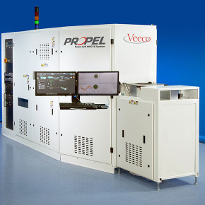
Propel Power GaN MOCVD System for Power Electronics. A Single-Wafer Reactor Technology to Enable Efficient, GaN-Based Power Devices (LINK)
 
"Our prior learning with Veeco's K465i GaN MOCVD system drove us to investigate the Propel HVM platform for our production ramp," said Marnix Tack, senior director of corporate R&D and open innovation at ON Semiconductor. 
 
"The beta test results demonstrated superior device performance with high uniformity and within-wafer and wafer-to-wafer repeatability, while meeting our cost-of-ownership targets for six- and eight-inch wafers. As such, the Propel HVM system proved to be the most suitable platform for our power electronics manufacturing needs."
 
The Propel HVM platform is based on Veeco's innovative single-wafer system with proprietary IsoFlange and SymmHeat technologies that provide homogeneous laminar flow and uniform temperature profile across the entire wafer. The system enables production of power electronics, laser diodes, radio frequency devices and advanced LEDs with higher performance and production yields while ensuring low cost of ownership.

Source: Photonics LINK

Tuesday, May 8, 2018

TSMC Details 5 nm Process Technology

At a special event last week, TSMC announced the first details about its 5 nm manufacturing technology that it plans to use sometime in 2020. CLN5 will be the company's second fabrication process to use extreme ultraviolet (EUV) lithography, which is going to enable TSMC to aggressively increase its transistor density versus prior generations. However, when it comes to performance and power improvements, the gains do not look very significant.Just like other fabs, TSMC will gradually ramp up usage of ASML's Twinscan NXE:3400 EUV step and scan systems. 
 
Next year TSMC will start using EUV tools to pattern non-critical layers of chips made using its second-gen 7 nm fabrication technology (CLN7FF+). Usage of EUV for non-critical layers will bring a number of benefits to the CLN7FF+ vs. the original CLN7FF process, but the advantages will be limited: TSMC expects the CLN7FF+ to offer a 20% higher transistor density and a 10% lower power consumption at the same complexity and frequency when compared to the CLN7FF. 
 
TSMC's 5 nm (CLN5) technology will increase the usage of EUV tools and this will bring rather massive advantages when it comes to transistor density: TSMC is touting a 1.8x higher transistor density (~45% area reduction) when compared to the original CLN7FF, but it will only enable a 15% frequency gain (at the same complexity and power) or a 20% power reduction (at the same frequency and complexity). With the CLN5, TSMC will also offer an Extremely Low Threshold Voltage (ELTV) option that will enable its clients to increase frequencies of their chips by 25%, but the manufacturer has yet to describe the tech in greater detail.The rather small, incremental improvements that TSMC is discussing for the CLN7FF to CLN7FF+ and CLN7FF+ to CLN5 transitions indicate that it gets increasingly harder to offer decent gains from generation to the next. It remains to be seen whether all of TSMC's leading-edge customers will keep adopting all the latest process technologies that the company offers, or will miss certain cycles given small incremental increases, but large companies (such as Apple) adopted all the latest fabrication processes in the recent years (i.e., it made economic sense to adopt them). 
 
Source: AnandTech LINK

Picosun aims for even stronger growth with bridge financing while preparing to be listed

ESPOO, Finland, 8th May, 2018 – Picosun Group, a leading provider of ALD (Atomic Layer Deposition) thin film coating technology for global industries, has decided of minimum one and a half million euros’ increase of the share capital in its Extraordinary General Meeting. This sum, coming from the existing shareholders, is a part of minimum five million euros’ bridge financing.

”We have invested a lot of money in research and development, which shows now in extremely strong growth. With the bridge financing we enable acceleration of this growth while preparing to be listed,” says Mr. Kustaa Poutiainen, Chairman of the Board and CEO of Picosun Group.

In the previous fiscal year, which ended 30th September 2017, Picosun’s turnover grew 28 percent to 18.9 million euros. During the first half of the current fiscal year the growth increased to 61 percent.

The growth continues, as in the end of March 2018 the value of Picosun’s 12 month cumulative received new orders was 27.8 million euros. As of today, the company’s order backlog is worth 11 millions. At the same time, Picosun has improved its profit.

”We have earned the trust of also our big, industrial customers, which is why especially our repeat sales have grown. We will always take good care of our R&D, agility, and fulfilling our customers’ needs,” Poutiainen continues.

In the first half of the current fiscal year Picosun’s net profit was 1.2 million euros.

ALD is a Finnish invention, patented by Dr. Tuomo Suntola already in 1974. Suntola is a Picosun Board Member and one of the owners of the company.

Ultra-thin and pinhole-free films deposited with Picosun’s ALD equipment cover perfectly even three-dimensional surfaces. ALD technology is a necessity in microelectronics and LED industries and in manufacturing protective coatings on various objects.

The use of ALD expands fast, as new applications emerge all the time.

”We are especially excited when the new financing enables us to help also the health industries to develop. Picosun has developed ALD coating solutions for e.g. surgical implants and medicines, and our customers are already using these solutions in their production. We believe that ALD can give a giant boost to health industries, just like it did to electronics industry,” states Poutiainen.

Monday, May 7, 2018

Veeco Instruments reports revenue jumped to $158.6 million in 1Q/2018

Veeco Instruments Inc. Monday reported a jump in first-quarter revenue driven in part by strong demand for its equipment used in producing light-emitting diodes. The Plainview company had revenue of $158.6 million for the quarter ended March 31. That compared wuth revenue of $94.5 million in the 2017 period.

John R. Peeler, Veeco's chairman and chief executive, in a statement, attributed the revenue growth to shipments of specialized lithography systems and equipment used in producing LEDs. The company posted a net loss of $15.8 million, or 34 cents per share, versus net income of $1.6 million, or 4 cents a share in the 2017 period.

Source: Newsday LINK

Aixtron: VPEC expands capacities with Aixtron technology

Taiwanese epi foundry, Visual Photonics Epitaxy Co. Ltd. (VPEC), chooses Aixtron MOCVD systems to meet growing demand for lasers and other devices.
Aixtron will deliver all AIX 2800G4 reactors with an 8x6-inch wafer configuration for maximum yield at high quality levels.

“Aixtron is the leading provider of high-volume manufacturing equipment for arsenide phosphide (AsP) based materials. As a proven tool for high-volume production in the area of photonic applications, the AIX 2800G4 system delivers exactly the outstanding uniformity and reproducibility, but also flexibility and versatility that we require as an epi foundry to serve the needs of our demanding customers,” Neil Chen, Senior Vice President of VPEC, says in the release.

“Driven by the growing number of applications and the continuing penetration of high-end communication technology, the demand for arsenide phosphide based optoelectronic devices such as VCSELs or datacom lasers is expected to increase further. Based on a longstanding and trustful relationship with VPEC, we are looking forward to support the growth of one of the leading epi foundries in Asia”, says Dr. Bernd Schulte, President of Aixtron SE.

Source: Evertiq LINK

Friday, May 4, 2018

TSMC ramps 7nm and details technology roadmap including EUV for early 2019

[EE Times] TSMC announced that it is in volume production with a 7-nm process and will have a version using extreme ultraviolet (EUV) lithography ramping early next year. In addition, it gave its first timeline for a 5-nm node and announced a half-dozen new packaging options.
TSMC is in volume production of 7-nm chips today with more than 50 tapeouts expected this year. It’s making CPUs, GPUs, AI accelerators, cryptocurrency mining ASICs, networking, gaming, 5G, and automotive chips.

The node delivers 35% more speed or uses 65% less power and sports a 3x gain in routed gate density compared to the 16FF+ generation two steps before it. By contrast, the N7+ node with EUV will only deliver 20% more density, 10% less power, and apparently no speed gains — and those advances require use of new standard cells.

Full article : EE Times LINK 
According to TSMC, their 7nm Fin Field-Effect Transistor (FinFET) process technology provides the industry's most competitive logic density and sets the industry pace for 7nm process technology development by delivering 256Mb SRAM with double-digit yields in June 2016. Risk production started in April 2017.
TSMC's 7nm Fin Field-Effect Transistor (FinFET) process technology [TSMC.com]

TSMC's 5 nm and a the later version of 7 nm FinFET will adopt EUV Lithography for more critical layers to reduce multi-pattern process complexity while achieving aggressive die area scaling. 
As reported in April, Intel has pushed out their 10 nm node to some time in 2019 due to yield issues in multiple patterning (LINK). The Intel 10 nm is comparable in transistor density too the Foundry 7 nm nodes (see graph below), which mean that by this announcement TSMC has taken over the lead from Intel in scaling.
Intel's Mark Bohr also declared the standard node inadequate and proposed that transistor density be used as a metric instead. However, Scotten Jones has calculated transistor densities for the manufacturers' processes using the Intel definition. When these are plotted against standard nodes, the densities are exactly what one would expect from the standard node values. The Intel transistor densities are values disclosed by Intel, rather than calculated. [Seeking Alpha, LINK]