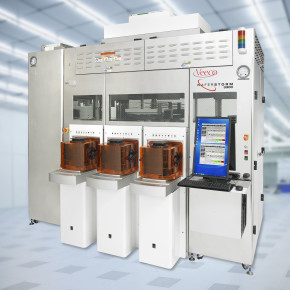
Showing posts with label Veeco. Show all posts

Tuesday, September 10, 2019

WZW-Optic AG orders multiple Veeco optical coating systems

WZW-Optic AG to Leverage Veeco’s SPECTOR®Systems—the Market’s Lowest-Loss Laser Optical Coating System—for Manufacturing Navigational Equipment 

Plainview, N.Y., Sept. 10, 2019—Veeco Instruments Inc. (Nasdaq: VECO) today announced that WZW-Optic AG, a Swiss leader in manufacturing high-end optics and precision optical components, has ordered multiple Veeco SPECTOR Ion Beam Sputtering (IBS) optical coating systems. WZW will leverage Veeco’s proven IBS technology, which produces the lowest optical loss films in the market, to manufacture high-performance laser mirrors for a range of applications, including ring laser gyroscope mirrors used for commercial aviation. These systems were sold in cooperation with Veeco’s channel partner in France, veonis Technologies EURL.

“For over 50 years, we’ve manufactured the highest quality optics solutions for customers around the globe,” said Claudio Meli, CEO, WZW. “Ultra high-end optics demand coatings with greater precision than ever before, and our selection of Veeco’s industry-proven SPECTOR systems ensures we can deliver superior quality coatings at the lowest optical loss level in the industry.”


According to Adroit Market Research the optical coatings market is expected to hit $25 billion by 2025, led by the advent of 5G, autonomous driving technology and an increased number of fiber networks using optical coatings. This has created a need for IBS systems like the SPECTOR platform that can achieve highly productive levels of precision and thin film process flexibility. As Veeco customers report, SPECTOR is a turn-key solution for meeting the yield and device performance requirements for virtually every high-end optical thin film fabrication application today.

“With over 300 tools in production worldwide, Veeco proudly has one of the largest installed bases of IBS tools for precision optics in the industry,” added Adrian Devasahayam, Ph.D., Senior Vice President, Product Line Management. “As the recognized leader in providing optical coating technology, we are confident that our SPECTOR systems will be a significant differentiator for WZW, a key supplier for high-end optical components.”


Wednesday, April 3, 2019

VEECO Demonstrates Thought Leadership at Technical Conferences in 2Q/2019


Company’s Technologists to Present Innovations that Drive Industrial Scaling of Technology Megatrends in Big Data, Artificial Intelligence, Communications, Autonomous Vehicles, Displays and More

PLAINVIEW, New York, April 2, 2019—Veeco Instruments Inc. (Nasdaq: VECO) today announced its leading technologists are scheduled to speak at seven technical events throughout Q2 2019. The forthcoming presentations, which follow several notable appearances in Q1, highlight Veeco’s depth and breadth of expertise in working with customers to break through production-scale barriers that will ultimately lead to the wide adoption of game-changing trends in big-data, high-speed communications, artificial intelligence, autonomous vehicles, high resolution displays and more.

Veeco exhibiting and presenting at EFDS ALD for Industry (March 19-20; Berlin, Germany) “Atomic Layer Deposition Use for Decorative Applications” Ganesh Sundaram, Ph.D., vice president of Applied Technology, Veeco CNT. (Photo by Martin Knaut LINK)

Through these papers, Veeco explains how it solves tough materials engineering challenges with advances in its deposition, etch, lithography and wet processing technologies used in applications such as next-generation advanced packaging, photonics, sensors, MEMS, micro-LEDs, power electronics, high bandwidth memory and related devices. Presentations in the second quarter include:

  • MRS Spring Meeting & Exhibit (April 22-26; Phoenix, AZ)—Tania Henry, process development engineer, will present “Influence of Intermixing on Perpendicular Magnetic Anisotropy of Ion-Beam-Deposited CoFeB MTJs for STT-RAM,” on April 25 during the annual meeting focused on the future of materials science
  • Critical Materials Council Conference (April 25-26; Saratoga Springs, NY)—Drew Hanser, vice president of technology, will present at the fourth annual forum for discussing actionable information related to semiconductor fab materials. Hanser’s talk, “Material Integration Challenges for GaN on Si for Power and RF Devices,” takes place on April 25 during Session II: Immediate Challenges of Materials & Manufacturing
  • Society of Vacuum Coaters TechCon (April 27-May 2; Long Beach, CA)—At one of the world’s leading vacuum coating technology conferences, senior research scientist Binyamin Rubin will discuss “Monochromatic and Broadband Optical Monitoring for Deposition of Band Pass Filters,” on April 29. The Veeco team will also be exhibiting its latest advances in ion beam deposition systems for optical coatings at booth #229
  • CS ManTech (April 29-May 2; Minneapolis, MN)—Phillip Tyler, process development engineer, will present “Development of Advanced Lift Off Processes for 5G and VCSEL Applications.” Stop by Veeco’s booth #609 to learn more about the company’s latest innovations in compound semiconductor and wet processing technologies
  • ECTC (May 28-31; Las Vegas, NV)—Dr. Ajit Paranjpe, chief technology officer, will co-author a presentation on “High-Yield Precision Transfer and Assembly of Gallium Nitride (GaN) Micro-LEDs Using Laser Assisted Micro Transfer Printing,” with experts from the University of California, Los Angeles
  • EUVL Workshop (June 10-13; Berkeley, CA)—At this year’s workshop focused on the fundamental science of EUV lithography and its continued extension to support Moore’s Law, Sandeep Kohli, principal research scientist, will present “Ion Beam Technology Roadmap for EUV Mask Deposition and Absorber Etch Processes”
  • TechConnect World Innovation Conference and Expo (June 17-19; Boston, MA)—Dr. Ganesh Sundaram, vice president of applied technology, will present “Atomic Layer Deposition for Life Science Applications” on June 17 at the Nanomedicine Symposium
Veeco scientists also presented research at a number of key technical conferences in Q1, including:
  • SPIE Advanced Lithography (Feb. 24-28; San Jose, CA)
    • “Ion Beam Etching of Advanced Absorber Materials for Sub-5nm EUV Masks”
    • “Intra-field Stress Impact on Global Wafer Deformation” (alongside ASML and imec)
  • EFDS ALD for Industry (March 19-20; Berlin, Germany)
    • “Atomic Layer Deposition Use for Decorative Applications”
  • CS International (March 26-27; Brussels, Belgium)
    • “Accelerating Photonics Growth through Advances in High-Performance Arsenic/Phosphide (As/P) MOCVD and Wet Processing Technology”
“Veeco builds production-scale fab solutions that solve tough materials engineering problems for our customers,” said Ajit Paranjpe, Ph.D., chief technology officer. “Our technical contributions to these prestigious and peer-reviewed conferences demonstrate Veeco’s commitment to remaining at the forefront of technological advances, which ultimately have a positive impact on society through life-improving applications.”

About Veeco

Veeco (NASDAQ: VECO) is a leading manufacturer of innovative semiconductor process equipment. Our proven MOCVD, lithography, laser annealing, ion beam and single wafer etch and clean technologies play an integral role in producing LEDs for solid-state lighting and displays, and in the fabrication of advanced semiconductor devices. With equipment designed to maximize performance, yield and cost of ownership, Veeco holds technology leadership positions in all these served markets. To learn more about Veeco's innovative equipment and services, visit www.veeco.com.

Saturday, March 23, 2019

Aledia Taps Veeco's Compound Semiconductor Expertise, Citing High-Quality Gallium Nitride Epitaxial Film Performance

Display Technology Innovator Expands Portfolio of Veeco Thin Film Process Technologies to Advance Next-Generation 3D Micro-LEDs

PLAINVIEW, New York, — Veeco Instruments Inc. (Nasdaq: VECO) announced today that Aledia, a developer and manufacturer of next-generation 3D LEDs for display applications, has expanded its portfolio of Veeco thin film process equipment to support the development and production of advanced 3D micro-LEDs. Aledia cited Veeco’s proven leadership in compound semiconductor applications, GaN-on-silicon growth performance, and capability to grow a full range of high-quality epitaxial films as key factors influencing its decision. 
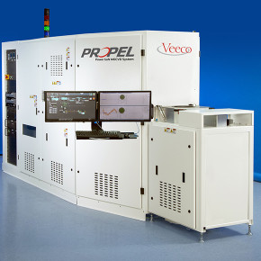
Veeco’s Propel™ Power GaN MOCVD system is designed specifically for the power electronics industry. Featuring a single-wafer reactor platform, capable of processing six- and eight-inch wafers, the system deposits high-quality GaN films for the production of highly efficient power electronic devices.

“We have been impressed with the performance of Veeco’s Propel™ GaN MOCVD platform for large-wafer 3D LED production, and naturally turned to Veeco again to support our advanced LED development,” said Philippe Gilet, co-founder and CTO of Aledia. “Veeco’s solutions meet our rigorous material quality and system delivery requirements along with unmatched material flux stability and repeatability. We are excited to take the next step with them in producing next-generation 3D micro-LEDs.”

The collaboration between Aledia and Veeco reflects the immense promise of micro-LEDs and other advanced LEDs for the future of displays. Micro-LEDs offer high efficiency, brightness and reliability benefits with shorter response time, enabling lighter, thinner and flexible displays with energy saving advantages for applications such as wearables, smartphones, automotive, signage/large TVs, augmented reality/virtual reality, etc. According to a recent Yole Développement report, there have been close to 1,500 patents filed related to micro-LED display from 125 different companies, with the bulk of activity occurring after 2012.

“With the significant shift toward exploration of micro-LEDs for use in next-generation displays, leaders like Aledia are turning to Veeco,” said Gerry Blumenstock, senior vice president and general manager of Veeco’s compound semiconductor business unit. “Veeco’s proven materials engineering expertise puts us in a unique position to offer innovative thin film deposition technologies for customers tackling tough compound semiconductor research, development and production challenges.”

Veeco will exhibit and present at the CS International Conference, March 26-27, 2019 in Brussels, Belgium. Mark McKee, director of product marketing for Veeco’s MOCVD business unit, will present “Accelerating Photonics Growth through Advances in High Performance As/P MOCVD and Wet Processing Technology,” on March 27, 2019 at 9:50 a.m. CET.

Friday, March 1, 2019

Skywater Technology Foundry selects Veeco´s Waferstorm for 3D Monolithic SoC development


PLAINVIEW, N.Y., Feb. 28, 2019—Veeco Instruments Inc. (NASDAQ: VECO) today announced that SkyWater Technology Foundry has taken delivery of the WaferStorm® single wafer wet process system to support advanced development work for the design and fabrication of next-generation 3D monolithic System-on-a-Chip (3DSoC) technology. One of the most advanced U.S.-based semiconductor technology foundries, SkyWater is leveraging the process performance and production capabilities of the WaferStorm to create densely integrated logic and memory products. Using breakthrough 3DSoC technology, the foundry is collaborating with researchers at the Massachusetts Institute of Technology (MIT) to set a new threshold for device performance and energy efficiency.

 
“Our selection of the WaferStorm system was based on Veeco’s track record of delivering best-in-class technology for wet processing that enables many leading-edge applications,” stated Thomas Sonderman, president of SkyWater. “The solvent-based platform offers a precise level of control during wafer processing, which is essential to the innovations we are working on with MIT to develop technology that drives better performing devices at lower cost.”

WaferStorm’s unique ImmJET™ solvent technology provides customers with the best overall process performance, flexibility and production capability in its class compared to conventional batch or spray-only approaches. WaferStorm offers proven, reliable solutions for metal lift-off (MLO), photoresist strip, dry film resist strip, via cleans, flux removal and other advanced packaging processes. WaferStorm is also the production tool of record for MLO at several leading vertical-cavity surface-emitting laser (VCSEL) manufacturers today.

“SkyWater’s selection of the WaferStorm further showcases Veeco’s leadership in advanced wet processing technology, and we’re pleased to be working with the renowned foundry that is driving true innovation in the 3DSoC space,” said Scott Kroeger, general manager of Veeco’s Precision Surface Processing business unit. “Our full suite of solvent, clean and etch technologies is ideally suited to help create a new class of microelectronic devices and systems that extends beyond previous thresholds for performance and efficiency.” As reported by IEEE, advances in monolithic 3D integration lay the foundation for highly efficient next-generation computing systems. With the emergence of artificial intelligence, edge computing and deep learning driving innovation in memory access as a key enabler for future systems design, the use of 3DSoC represents a paradigm shift for the computer industry and high-tech world. As the industry reaches the next-generation of 3DSoC technology, WaferStorm delivers excellent process results at the lowest cost of ownership, enabling innovators like SkyWater and MIT to advance research and enhance device performance.

Sunday, February 10, 2019

Fraunhofer Institute for Telecommunications to Receive Veeco’s SPECTOR® Ion Beam Sputtering System with Enhanced Sirius™ Optical Monitoring System


Plainview, N.Y., Feb. 5, 2019 – Veeco Instruments Inc. (Nasdaq: VECO) announced today that it has shipped its SPECTOR® Ion Beam Sputtering (IBS) system and the Sirius™ Optical Monitor System (OMS) to Fraunhofer Institute for Telecommunications. Fraunhofer, based in Berlin, will use Veeco’s IBS technology to develop and produce laser facet coatings and other micro-optical devices.

“The development of sophisticated micro-optical devices requires exceptional sputtering technology,” said Ms. Greta Ropers, head of backend and packaging group for Fraunhofer. “Veeco’s SPECTOR system, coupled with the Sirius OMS, ensures we are developing and producing world-class devices with the highest throughput and process repeatability on an automated, proven platform.”

According to customers, the SPECTOR platform generates the highest quality optical thin films with improved levels of productivity and throughput. Unlike evaporative coatings, ion beam sputtered thin films are deposited at high energies, giving exceptional thickness control and low defect densities for laser coating applications. Veeco’s Sirius OMS significantly enhances the SPECTOR platform capability by coupling cutting edge broadband monitoring control with the inherent stability of ion beam deposited films.

“Fraunhofer Institute for Telecommunications is a recognized worldwide leader in developing next generation laser facet coatings and micro-optical devices,” said Adrian Devasahayam, Ph.D., vice president and general manager of Veeco’s Advanced Deposition and Etch (AD&E) business. “The SPECTOR system sets the standard for precision optical coating thin films by providing unparalleled quality and flexibility that will no doubt accelerate their development goals.”

Funding for this project was granted by Forschungsfabrik Mikroelektronik, a cross-location research factory for microelectronics and nanoelectronics compromised of eleven institutes within the Fraunhofer Group along with the IHP GmbH - Innovations for High Performance Microelectronics and the Ferdinand-Braun-Institut, Leibniz-Institut für Höchstfrequenztechnik. For more information, please visit https://www.forschungsfabrik-mikroelektronik.de/en.html. The system was sold in cooperation with Veeco’s European channel partner, veonis Technologies GmbH.

Veeco is exhibiting at Photonics West (Feb. 5-7, San Francisco) and encourages attendees to visit Booth #3202 to learn more. Technical experts will discuss latest innovations in optical coating technology for industrial, defense, medical and telecom applications and MOCVD solutions for 3D sensing, LiDAR and datacom applications.


Thursday, January 10, 2019

Leading Provider of Semiconductor Manufacturing Services Selects Veeco's AP300 to Support Aggressive Advanced Packaging Expansion

World’s Largest OSAT Provider Names AP300™ Its Preferred Lithography System Due to Veeco’s Industry-Leading Uptime and Process Performance

PLAINVIEW, New York, Jan. 8, 2019 — Veeco Instruments Inc. (Nasdaq: VECO) announced today that the world’s largest outsourced assembly and test (OSAT) provider has purchased multiple Veeco AP300™ lithography systems. Complementing the OSAT’s previously installed Veeco tools, the AP300 was selected based on its industry-leading uptime and performance with lower total cost of ownership (CoO). This purchase is illustrative of continued strong market demand for Veeco’s lithography systems, given the tools’ ability to handle next-generation advanced packaging process needs including copper (Cu) pillar, wafer-level packaging (WLP), fan-out WLP (FOWLP) and 3D integrated circuit developments.

The AP300 lithography stepper’s winning combination of overlay, resolution, sidewall profile performance and broadband flexibility enables highly automated, cost-effective manufacturing valued by foundries and OSATs for applications such as fan-in WLP, FOWLP, through-silicon via, silicon interposer solder and Cu pillar bumping. Given the strong market growth expected in mobile, IoT and artificial intelligence (AI) applications, OSATs seek to ensure they are competitively positioned to drive customer acquisition and retention. According to Yole, the equipment and materials market for FOWLP alone will expand at a compound annual growth rate (CAGR) of 43 percent to reach $694 million by 2021.

“Increased mobility, IoT, AI and deep learning are seeing strong growth in step with global megatrends, all of which are enabled by technologies like 3D integration and advanced packaging,” noted Peter Porshnev, Ph.D., senior vice president and general manager of Veeco’s Ultratech business unit. “As we grow our customer base, Veeco’s experienced team of technologists continues to work closely with OSATs and foundries to deliver industry-leading innovations that directly address their performance, yield and CoO challenges.”

About Veeco

Veeco (NASDAQ: VECO) is a leading manufacturer of innovative semiconductor process equipment. Our proven MOCVD, lithography, laser annealing, ion beam and single wafer etch and clean technologies play an integral role in producing LEDs for solid-state lighting and displays, and in the fabrication of advanced semiconductor devices. With equipment designed to maximize performance, yield and cost of ownership, Veeco holds technology leadership positions in all these served markets. To learn more about Veeco's innovative equipment and services, visit www.veeco.com.

Wednesday, December 19, 2018

The semi equipment market will contract 2019 but grow 20.7 percent to reach an all-time high 2020

TOKYO – December 12, 2018 – Releasing its Year-End Total Equipment Forecast at the annual SEMICON Japan exposition, SEMI, the global industry association representing the electronics manufacturing supply chain, today reported that worldwide sales of new semiconductor manufacturing equipment are projected to increase 9.7 percent to $62.1 billion in 2018, exceeding the historic high of $56.6 billion set last year. The equipment market is expected to contract 4.0 percent in 2019 but grow 20.7 percent to reach $71.9 billion, an all-time high. [Source: SEMI LINK] 

 
For 2019, SEMI forecasts that South Korea, China, and Taiwan will remain the top three markets, with all three regions maintaining their relative rankings. Equipment sales in South Korea is forecast to reach $13.2 billion, in China $12.5 billion, and in Taiwan $11.81 billion. Japan, Taiwan and North America are the only regions expected to experience growth next year. The growth picture is much more optimistic in 2020, with all regional markets expected to increase in 2020, with the market increasing the most in Korea, followed by China, and Rest of World [Source: SEMI LINK]

After a period of record growth in 2017-18, the semiconductor equipment industry is expected to face a slowdown in 2019. Logic is strong but memory is weak, and the trade issues between the United States and China are a cause for concern. According to a report in Semiengineering (LINK), heading into 2019, there is a shortfall of 200 mm equipment. The industry requires from 2,000-3,000 new or refurbished 200 mm tools to meet fab demand, according to SurplusGlobal. But there are only 500 available 200 mm tools on the market, according to the company. 200 mm tool prices will remain high. 300 mm tool prices are lower than 200 mm tool prices these days
 
For the ALD OEM market the situation is therefore heating up even though the. Currently the top 300 mm ALD equipment companies (ASM, TEL, Lam, Jusung, Wonik IPS, Applied Materials) does not actively support the market with pure play 200 mm products except for Large Batch Furnaces. So if you want a 200 mm single wafer ALD tool today you can buy a 300 mm tool and equip it with 200 mm handling or go to one of the smaller companies like Picosun, Veeco, Beneq, Oxford Instruments, which all have 200 mm ALD cluster products on the market today.
 
 
From presentation "ALD/CVD applications, equipment and precursors in high volume manufacturing" at SEMICON Europa 2018, available on SlideShare LINK.
----
Written by Abhishekkumar Thakur and Jonas Sundqvist


Friday, November 30, 2018

Gooch & Housego Installs Veeco’s IBS System for Advanced Optical Coating Capabilities


PLAINVIEW, New York—Nov. 29, 2018—Veeco Instruments Inc. and Gooch & Housego (G&H), the world’s leading supplier of high quality superpolished optical components today announced the successful installation of Veeco’s SPECTOR® Ion Beam Sputtering (IBS) Optical Coating System at G&H’s Moorpark, Calif. facility. The new capability provided by SPECTOR supports G&H’s expanding portfolio of high-quality optics for ultraviolet, visible and infrared systems used in telecommunications, aerospace and defense, life science and industrial applications.

SPECTOR offers exceptional layer thickness control, enhanced process stability and the lowest published optical losses in the industry, and has become the IBS system of choice for over 200 advanced manufacturing settings worldwide. G&H will use this system to support its expanding portfolio of high-quality optics for UV, visible and infrared systems used across telecommunications, aerospace and defense, life science and industrial applications. 
 
“G&H is at the forefront of engineering a broad range of photonics technologies, leveraging optical coatings to advance crystal growth, electro-optics and fiber optics in next-generation applications,” said Adam Morrow, product line manager at G&H. “As we navigate the increasingly complex specifications required for these processes, we’ve turned to Veeco as a partner that can uphold our long-standing pedigree of high-quality optics.”

G&H’s growing presence in the laser optics landscape builds on the company’s tenured history as a supplier of high-quality photonics components. Complementing G&H’s superpolished surfaces, Veeco offers IBS coatings that achieve very low levels of total loss while maintaining surface roughness quality, density and exceptional environmental stability.


The SPECTOR IBS platform offers exceptional layer thickness control, enhanced process stability, and the lowest published optical losses in the industry. The system is engineered to improve key production parameters, such as target material utilization, optical endpoint control, and process time for cutting-edge optical coating applications. The SPECTOR platform, which is the preferred IBS system in the industry, has been installed in more than 200 advanced manufacturing settings across the world.


“Veeco’s IBS systems allow our customers to achieve the highest precision and thin film process flexibility necessary for successful advanced photonics and next-generation high-growth applications,” added Adrian Devasahayam, Ph.D., vice president and general manager of Veeco’s Advanced Deposition and Etch (AD&E) business. “We’re confident in the SPECTOR system’s ability to provide G&H with the qualitative advantages of IBS technology, including low scatter loss, high film purity, stable deposition rates and film thickness control of less than 0.1 nm in a robust package that significantly boosts throughput and lowers cost of ownership for customers.”


According to BCC Research, the global market for optical coatings is expected to reach $14.2 billion in 2021, up from $9.5 billion in 2016. Key drivers of this growth are emerging applications in commercial and consumer categories, as well as innovative coatings to improve a broad range of existing applications.

Friday, November 9, 2018

Veeco and ALLOS Collaborate to Advance microLED Tech

Plainview, N.Y., Nov. 8, 2018—Veeco Instruments Inc. (Nasdaq: VECO) and ALLOS Semiconductors GmbH announced today the completion of another phase of their mutual effort to provide the industry with leading GaN-on-Silicon epiwafer technology for microLED production. The purpose of the companies’ most recent collaboration was to demonstrate the reproducibility of ALLOS’ 200 mm GaN-on-Si epiwafer technology on Veeco’s Propel® MOCVD reactor when producing epiwafers for many prominent global consumer electronics companies.

“To bring microLED technology into production, simply presenting champion values for a single metric is insufficient. It is essential to achieve the whole set of specifications for each wafer with excellent repeatability and yield,” said Peo Hansson, Ph.D., senior vice president and general manager of Veeco’s Compound Semiconductor business unit. “This successful joint effort reaffirms the power of combining Veeco’s superior MOCVD expertise with ALLOS’ GaN-on-Silicon epiwafer technology to provide customers a novel, proven and reliable approach to accelerate microLED adoption.” 


Tuesday, November 6, 2018

Leading Provider of Semiconductor Manufacturing Services Selects Veeco's AP300E to Support Aggressive Advanced Packaging Expansion


One of the World’s Largest Outsourced Assembly and Test Providers Names AP300E™ Their Preferred Lithography System Due to Veeco’s Industry-Leading Uptime and Process Performance

Nov. 06, 2018—Veeco Instruments Inc. (Nasdaq: VECO) announced today that one of the world’s largest outsourced assembly and test (OSAT) providers has purchased multiple Veeco AP300E lithography systems. Complementing the OSAT’s previously installed Veeco tools, the AP300E was selected based on its superior uptime, lower total cost of ownership (CoO) and exceptional performance. This purchase is illustrative of continued strong market demand for Veeco’s expanding portfolio of lithography systems, given the tools’ ability to handle next-generation advanced packaging process needs including copper (Cu) pillar, wafer-level packaging (WLP), fan-out WLP (FOWLP) and 3D integrated circuit developments. 
 
 
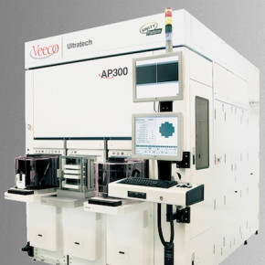
Veeco AP300, The AP200/300 family of lithography systems is built on Veeco’s customizable Unity Platform™, delivering superior overlay, resolution and side wall profile performance and enabling highly-automated and cost- effective manufacturing. These systems are particularly well suited for copper pillar, fan-out, through-silicon via (TSV) and silicon interposer applications (veeco.com).
The AP300E lithography stepper’s exceptional overlay, resolution, sidewall profile performance and broadband flexibility enable highly automated, cost-effective manufacturing valued by foundries and OSATs for applications such as fan-in WLP, FOWLP, through-silicon via, silicon interposer solder and Cu pillar bumping. Given the exponential market growth expected in mobile, IoT and artificial intelligence (AI) applications, OSATs seek to ensure they are competitively positioned to drive customer acquisition and retention. According to Yole, the equipment and materials market for FOWLP alone will expand at a compound annual growth rate (CAGR) of 43 percent to reach $694 million by 2021.

“Increased mobility, IoT, AI and deep learning are seeing explosive growth in step with global megatrends, all of which are enabled by technologies like 3D integration and advanced packaging,” noted Peter Porshnev, Ph.D., senior vice president and general manager of Veeco’s Ultratech business unit. “As we grow our customer base, Veeco’s experienced team of technologists continues to work closely with OSATs and foundries to deliver industry-leading innovations that directly address their performance, yield and CoO challenges.”

Friday, September 28, 2018

VEECO Ready to Provide Solutions for Micro LED Technology

 
As one of the most important next generation display technologies, Micro LED performs excellently and can be widely applied in wearables, mobile phones, automotive displays, AR/VR, video wall (digital display), TV and others. For solving the technology bottlenecks of Micro LED, the development of technology relies on cooperation between different companies with their expertise in equipment, materials, panels and brands.
 
Aside from the performance of products, LED manufacturers also need to consider their operation cost. Veeco has been helping them to reduce the cost of ownership with its equipment and has launched two sets of equipment, Propel enLight GaN MOCVD System and EPIK 868, for optimizing the operation to meet the demands of the market. Propel enLight GaN MOCVD System produces 200mm (8-inch) wafers and EPIK 868 produces 150mm (6-inch) wafers.

Source: LEDinside LINK

Tuesday, September 18, 2018

Veeco GEN10 Automated MBE Cluster System Wins Max Planck Institute Tender, Supporting Research of Oxide-Nitride Layer Structures

Prestigious Research Institute Cited Veeco’s Expertise in MBE and the High Reliability and Customization of the GEN10™ as Key Factors in its Decision

[Veeco, LINK] PLAINVIEW, N.Y., August 14, 2018—Veeco Instruments Inc. (NASDAQ: VECO) today announced that a dual chamber GEN10™ automated molecular beam epitaxy (MBE) cluster system won the tender offer by the Max Planck Institute of Microstructure Physics, Halle (Saale), Germany (MPI-MSP) to support world-class research on complex oxides. Demand for oxide-nitride layer structures has increased due to their enormous potential in enabling next-generation energy-efficient nano-devices and advanced data storage. The department of Nano-systems from Ions, Spins and Electrons (NISE) at the MPI-MSP will leverage Veeco’s MBE technology to expand research and develop innovative applications. 

Veeco's GENxplor R&D MBE System (Veeco.com)
“Our team is highly interested in exploring the properties of atomically engineered oxide-nitride layer structures especially because of their extraordinary properties but also for their potential in paving the way to novel energy-efficient nano-devices,” said Stuart Parkin, Director of the NISE Department at the MPI-MSP and Alexander von Humboldt Professor, Martin Luther University Halle-Wittenberg, Halle. “Veeco’s reputation and expertise in MBE combined with the GEN10’s high reliability, throughput, customization and automation capabilities will help support our research into novel materials.”

This win at MPI marks the first time Veeco has provided a fully integrated solution for a concentrated ozone source. The GEN10 allows for up to three configurable, material-specific growth modules, enabling high system utilization and allowing multiple researchers use the system at the same time to perform unattended growth. By expanding its reach in the R&D sector worldwide, Veeco is leading the way in helping grow complex oxide structures.

“As our MBE systems continue to expand their footprint in the global R&D space, we are honored that Veeco’s GEN10 MBE system was selected by the highly respected Max Planck Institute of Microstructure Physics in Halle,” noted Gerry Blumenstock, vice president and general manager of MBE and ALD products at Veeco. “We are pleased with the confidence Dr. Parkin and his team placed in our MBE expertise and we look forward to supporting the MPI-MSP as it continues to lead R&D exploration and applications for complex oxides.”

Tuesday, September 4, 2018

Veeco Announces Changes to Executive Leadership Team

PLAINVIEW, N.Y., September 4, 2018 —Veeco Instruments Inc. (NASDAQ: VECO) today announced that John Peeler, Chairman and Chief Executive Officer, will transition to the role of Executive Chairman, effective October 1, 2018. William J. Miller, currently President, will become Chief Executive Officer and will join the Company’s board of directors bringing the size of the board to eight. Additionally, Shubham (Sam) Maheshwari will be named Chief Operating Officer and will continue in his role as Chief Financial Officer. 

Peeler joined Veeco in 2007 as Chief Executive Officer and became Chairman of the Board in 2012. As Executive Chairman, Peeler will work closely with Miller and the Board to ensure an effective transition of management.

“With his impressive background and track record of notable achievements across strategic, product development and operational assignments, there is no one better suited than Bill to take over the helm as Veeco looks forward to its next chapter,” stated Peeler. “Bill and the executive team have the industry experience to execute Veeco’s vision while remaining committed to enabling tomorrow’s technology breakthroughs.”

Monday, July 9, 2018

Leading memory chip manufacturer purchases multiple VEECO AP300 lithography systems for DRAM interconnect applications

Growing Demand for Advanced Packaging in the Memory Market Highlights Value of Veeco’s
High Volume Manufacturing Lithography Systems


PLAINVIEW, New York, July 9, 2018 – Veeco Instruments Inc. (Nasdaq: VECO) today announced that one of the world’s leading memory chip manufacturers has ordered multiple AP300™ lithography systems to support the fast growing demand for DRAM with copper (Cu) pillars. The company selected the Veeco tools for their versatility in addressing advanced packaging applications, proven reliability in supporting high volume manufacturing and low total cost of ownership. 
This approach echoes a larger industry trend, with more and more memory manufacturers exploring the use of Cu pillars in DRAM interconnect applications due to their higher input/output (I/O) density, improved electrical performance and better thermal efficiency. “Within the DRAM market, the interconnect is shifting from wire bond to flip chip,” said Jan Vardaman, president of semiconductor packaging analyst firm TechSearch International, Inc. “We project that over the next three years, the annual number of flip chip interconnects in DRAM will grow 29 percent on a unit volume basis.”

The AP300 is part of a family of lithography systems built on Veeco’s customizable Unity Platform™, which delivers superior overlay, resolution and side wall profile performance, driving highly automated, cost-effective manufacturing for customers. The system is particularly well suited for Cu pillar, fan-out, through-silicon via (TSV) and silicon interposer applications. A low risk, low cost, high volume manufacturing solution, the AP300 is staged to support rapid market adoption of advanced packaging applications among memory manufacturers.

“The growing demand for innovative, alternative solutions to wire bonding in memory presents a strong opportunity for Veeco,” said Rezwan Lateef, vice president and general manager of lithography products at Veeco. “Furthermore, this significant customer adoption validates the AP300’s ability to address advanced packaging applications in a broader high-volume production market. To meet this demand, we are strengthening our regional technical staff to support numerous memory manufacturers looking to fast-track adoption.”

Veeco will be at Booth #6070 at SEMICON West in San Francisco, CA, July 10-12, 2018.

Friday, May 25, 2018

Veeco Instruments: Veeco's revenue grows 14% in Q1 to $158.6m, driven by MOCVD system shipments to China

For first-quarter 2018, epitaxial deposition and process equipment maker Veeco Instruments Inc of Plainview, NY, USA has reported a seventh consecutive quarter of revenue growth, to $158.6m (well above the midpoint of the $140-165m guidance). This is up 14% on $139.7m last quarter (adjusted from $143.4m after adopting the ASC 606 revenue recognition standard on 1 January) and up 68% on $94.5m a year ago.

“2018 is off to a great start with strong sequential and year-over-year revenue growth,” says chairman & CEO John R. Peeler. “Sales growth in the first quarter was driven primarily by shipments of our lithography systems into the advanced packaging market, and shipments of MOCVD systems for LED applications.”

Of total revenue, the LED Lighting, Display and Compound Semiconductor segment hence comprised 57%, growing to $90m, reflecting strong 2018 opening metal-organic chemical vapor deposition (MOCVD) backlog (delivering systems to five customers in China).

Source: Semiconductor Today LINK


Monday, May 21, 2018

Veeco Instruments: ON Semi Orders Veeco MOCVD System

ON Semiconductor Inc. has ordered the Propel High-Volume Manufacturing (HVM) Gallium Nitride (GaN) Metal Organic Chemical Vapor Deposition (MOCVD) system from Veeco Instruments Inc.
 
The Propel GaN MOCVD system is specifically designed for high-voltage power-management devices used in data centers; automotive, information and communication technology; defense; aerospace and power distribution systems, among other applications.
 

Propel Power GaN MOCVD System for Power Electronics. A Single-Wafer Reactor Technology to Enable Efficient, GaN-Based Power Devices (LINK)
 
"Our prior learning with Veeco's K465i GaN MOCVD system drove us to investigate the Propel HVM platform for our production ramp," said Marnix Tack, senior director of corporate R&D and open innovation at ON Semiconductor. 
 
"The beta test results demonstrated superior device performance with high uniformity and within-wafer and wafer-to-wafer repeatability, while meeting our cost-of-ownership targets for six- and eight-inch wafers. As such, the Propel HVM system proved to be the most suitable platform for our power electronics manufacturing needs."
 
The Propel HVM platform is based on Veeco's innovative single-wafer system with proprietary IsoFlange and SymmHeat technologies that provide homogeneous laminar flow and uniform temperature profile across the entire wafer. The system enables production of power electronics, laser diodes, radio frequency devices and advanced LEDs with higher performance and production yields while ensuring low cost of ownership.

Source: Photonics LINK

Monday, May 7, 2018

Veeco Instruments reports revenue jumped to $158.6 million in 1Q/2018

Veeco Instruments Inc. Monday reported a jump in first-quarter revenue driven in part by strong demand for its equipment used in producing light-emitting diodes. The Plainview company had revenue of $158.6 million for the quarter ended March 31. That compared wuth revenue of $94.5 million in the 2017 period.

John R. Peeler, Veeco's chairman and chief executive, in a statement, attributed the revenue growth to shipments of specialized lithography systems and equipment used in producing LEDs. The company posted a net loss of $15.8 million, or 34 cents per share, versus net income of $1.6 million, or 4 cents a share in the 2017 period.

Source: Newsday LINK

Wednesday, April 11, 2018

ON Semiconductor is going to HVM with Veeco Propoel MOCVD System for GaN Power devices

After Successful Beta Test, ON Semiconductor Selects Industry's First Single-Wafer Cluster Platform

PLAINVIEW, N.Y., April 10, 2018 (GLOBE NEWSWIRE) -- Veeco Instruments Inc. (Nasdaq:VECO) today announced that ON Semiconductor (Nasdaq:ON) has ordered its Propel® High-volume Manufacturing (HVM) Gallium Nitride (GaN) Metal Organic Chemical Vapor Deposition (MOCVD) system. Based on its successful beta evaluation of the Propel HVM tool, ON Semiconductor ordered the production-level Propel system for GaN power electronics manufacturing. As the industry's first single-wafer cluster platform, the Propel GaN MOCVD system is specifically designed for high-voltage power-management devices used in data centers; automotive, information and communication technology; defense; aerospace and power distribution systems, among other applications
'Our prior learning with Veeco's K465i™ GaN MOCVD system drove us to investigate the Propel HVM platform for our production ramp,' said Marnix Tack, PhD, senior director of corporate R&D and Open Innovation at ON Semiconductor. 'The beta test results demonstrated superior device performance with high uniformity and within-wafer and wafer-to-wafer repeatability, while meeting our cost-of-ownership targets for six- and eight-inch wafers. As such, the Propel HVM system proved to be the most suitable platform for our power electronics manufacturing needs.'

The Propel HVM platform is based on Veeco's innovative single-wafer system with proprietary IsoFlange™ and SymmHeat™ technologies that provide homogeneous laminar flow and uniform temperature profile across the entire wafer. The system enables production of power electronics, laser diodes, RF devices and advanced LEDs with higher performance and production yields while ensuring very low cost-of-ownership.

'The Propel HVM platform is rapidly gaining traction in the industry as innovative companies like ON Semiconductor recognize the benefits of GaN-on-silicon, which will partially replace current silicon technology for power electronics,' commented Peo Hansson, PhD, senior vice president and general manager of Veeco MOCVD operations. 'With its highly controlled doping, run-to-run stability, superior wafer uniformity, high productivity and uptime, Propel HVM extends the benefits of our TurboDisc® platform to a unique single-wafer architecture. These capabilities benefit customers that seek a superior solution for manufacturing while providing a path for scaling to eight-inch wafers and expansion to RF and other advanced applications.'

GaN is a wide band gap semiconductor material with specific advantages over conventional technologies such as gallium arsenide (GaAs) and silicon carbide (SiC). GaN has enormous potential in the short term due to its benefits in terms of thermal behavior, efficiency, weight and size. According to market research firm Yole Développement, the GaN power device business was worth $14 million in 2016, and projects that it will reach $460 million by 2022, with a compound annual growth rate (CAGR) of 79 percent. GaN-based devices will be used increasingly in RF amplifiers, LEDs and high voltage applications among others, primarily due to their abilities to operate at high frequency, power density and temperature with improved efficiency and linearity.

Veeco is discussing the power of its innovative MOCVD and wet etch systems in the '5G: Where Are We and What's Next?' track at the CS International Conference this week in Brussels, Belgium. Somit Joshi, senior director of MOCVD marketing is presenting a session titled, 'Enabling GaN RF and Power Electronics through Innovative MOCVD and Wet Etch Process Technologies,' on Wednesday, April 11, and the Veeco team will also be accepting the CS Industry 2018 Award for Innovation for its GENxcel™ R&D MBE System at the awards ceremony held during the conference.

Source: 4-traders LINK

Wednesday, March 28, 2018

Veeco touts 100 automated MBE systems installed worldwide


Plainview, NY. Veeco Instruments Inc. today announced it has completed installation of its 100th automated Molecular Beam Epitaxy (MBE) system. The installation of Veeco’s GEN10 MBE System last month at Silanna Semiconductor PTY Ltd. in Australia marks this company milestone. The company also operates a Veeco Dual GEN200 MBE System for production of advanced nitride compound semiconductor devices including ultraviolet LEDs (UV-LEDs).

“Veeco has earned a reputation for consistently developing innovative and reliable MBE technology from research scale to production,” said Petar Atanackovic, Ph.D., chief scientist of Silanna Semiconductor PTY Ltd. “The flexibility and deposition capability of the GEN10 system will enable us to develop new materials at the atomic level allowing us to exploit new quantum properties. Veeco’s technology portfolio and leadership in MBE systems provides us with a clear path to easily scale to volume production in the future.”

Source: Evaluation Engineering LINK

Friday, February 9, 2018

Cases Closed: Veeco, AMEC, and SGL Settle Patent Litigation


Veeco Instruments Inc., Advanced Micro-Fabrication Equipment Inc. (AMEC), and SGL Carbon SE (SGL), today announced that they have mutually agreed to settle the pending litigation among the parties and to amicably resolve all pending disputes, including AMEC's lawsuit against Veeco before the Fujian High Court in China and Veeco's lawsuit against SGL before the U.S. District Court for the Eastern District of New York.

Source: LEDinside LINK