Wednesday, March 8, 2017

REGISTER NOW FOR CRITICAL MATERIALS COUNCIL (CMC) CONFERENCE 2017


REGISTER NOW FOR CRITICAL MATERIALS COUNCIL (CMC) CONFERENCE 2017
The Critical Materials Council (CMC) Conference is a 2 day event, May 11-12 in Dallas, TX, providing actionable information on materials and supply-chains for current and future semiconductor manufacturing. Notable speakers from leading IDMs such as Intel and Micron, materials companies, and market research firms will provide insights on the ever changing area of semiconductor process materials and markets.

Keynote speaker Dr. Hans Stork, SVP & CTO of ON Semiconductor, will start the event with sessions covering:
  • Updates on Semiconductor Materials Market Dynamics and Government Regulations
  • Conflict Minerals & Supply Chain Issues
  • Material Handling Issues Cradle to Grave and
  • Metrologies Needed for Profitable Control of All Critical Materials
  • ALD Precursor Purification to CMP Slurries.
For more information and registration go to http://cmcfabs.org/cmc-events/.

Webinar on Atomic Layer Deposition (ALD) Market Analysis

Description

A Webbinat by IndustryARC Nearly the last 5 decades have witnessed Atomic Layer Deposition successfully applied in the growth of thin films of many classes of materials, including metal oxides, metals, polymers, and inorganic-organic hybrid materials. ALD has paved its way across a large section of industries be it medical or biological or semiconductor or for laboratory purposes. While the development of biosensors, drug delivery devices and implants lead the lifesciences domain; manufacturing of electronic circuit components is one of the top most uses of ALD in the electronics segment.

Date and Time

Thu, March 23, 2017
7:30 PM – 8:30 PM SST
Registration: LINK

Samsung Relies on ALD for Continued Scaling of DRAM for 10nm Class Technology:

With DRAM memory, where each cell consists of a capacitor and a transistor linked to one another, scaling is more difficult than with NAND Flash memory in which a cell only needs a transistor. To continue scaling for more advanced DRAM, Samsung refined its design and manufacturing technologies and came up with a modified double patterning and atomic layer deposition.

The Fuel Cell and ALD Overhaul:

ALD has clearly gained prominence in manufacture of fuel cell. IndustryARC predicts high potential in this field in the coming years. Solid Oxide Fuel Cells are noted a quality contribution to the global ALD market:

Durable and high-performance low temperature solid oxide fuel cells
ALD of ultrathin blocking layer for low-temperature solid oxide fuel cell on nanoporous substrate

Supercapacitors Manufacturing: ALD to the Rescue?

With the invent of ALD, energy conversion, producing cost competitive, durable and high performance devices have become increasingly significant and one such application is manufacture of a supercapacitor! Manufacturers, developers and suppliers of supercapacitors have lately gained utmost ascendancy. ALD encapsulated activated carbon electrodes for high voltage stable supercapacitors- continue to trend in the market.

Sunday, March 5, 2017

Picosun Expands Services and Support with Retronix

Picosun Oy, the leading supplier of advanced industrial ALD (Atomic Layer Deposition) technology, announces collaboration with Retronix Semiconductor, a well-known and highly reputed global engineering service company, to further reinforce its support and service portfolio especially for production customers.

Picosun's industrial customer base is growing fast, with increasing number of high throughput, fully automated cluster and batch production tools installed worldwide at prominent semiconductor manufacturers. To ensure always first class support tailored to every customer's individual needs, Picosun provides an all-inclusive service selection with quick lead times and comprehensive, system-specific products with competitive pricing. The services range from 24/7 support and maintenance contracts and coating service to process consultancy and advanced training programs, provided by Picosun's own Ph.D level ALD scientists, highly qualified engineers, and the company's worldwide network of distributors and representatives.

To further strengthen this service portfolio, Picosun has now signed an agreement with Retronix Semiconductor. This ensures even faster response times with highest level support for a fast growing and increasingly demanding customer base. Picosun will also continue offering support locally through current representatives and its own personnel.

"Customer happiness is essential for us at Picosun. This calls not just for the best in class ALD tools with superb process quality, but unfaltering supply, support and service chain. This is particularly emphasized on production lines where the smallest issues can easily lead to massive financial losses. We are very pleased to start collaboration with Retronix as our world-wide service partner. Their workforce of highly trained and specialized service professionals complements our service section and guarantees even better customer experience", states Dr. Erik Ă˜streng, Applications and Services Director of Picosun.

Thursday, March 2, 2017

ASM International today reports its fourth quarter 2016 operating results

ASM International today reports its fourth quarter 2016 operating results (LINK)
  • Net sales for the fourth quarter 2016 were €173 million, an increase of 20% compared to the previous quarter. Year-on-year net sales increased with 19%.
  • New orders at €177 million were 44% above the Q3 2016 level.
  • Normalized net earnings for the fourth quarter 2016 increased by €29 million compared to the third quarter 2016. Operating result increased to €30 million. The financing result included €19 million positive effects from currencies compared to €3 million negative effects in the third quarter. The result from investments decreased with €8 million.


Commenting on the results, Chuck del Prado, President and Chief Executive Officer of ASM International said: "The strong overall market climate for semiconductor equipment towards the end of 2016 led to better sales and a higher order intake for Q4 than forecasted. The net cash position of ASMI remained strong. In addition to a stable proposed dividend of €0.70 per share, we announce today an increase in our current share buyback program from € 50 million to €100 million."

Outlook

  • Demand in the Logic/Foundry segment is expected to remain healthy.
  • We believe the 3D-NAND contribution to the single wafer ALD market will show a strong increase in 2017, leading to increased orders for ASMI.
  • The DRAM segment is expected to show a modest recovery in 2017.

We expect that the single wafer ALD market experienced a double digit decline in 2016. Based upon that we forecast the single wafer ALD market to reach a size of approx. US$1.5 billion in 2020-2021.

We project a year-on-year sales increase for the first half of 2017, whereby we expect a sales level of €135-145 million for Q1 and €160-200 million for Q2, both on a currency comparable level. The order intake in Q1 is expected to remain healthy at a level of €170-190 million, also on a currency comparable level.


Wednesday, March 1, 2017

ASM International has received a supplier excellence award from TSMC

ASM International reports: ASM International has received a supplier excellence award as one of five equipment suppliers from TSMC for the performance and support of ASM's ALD equipment and technology during 2016. The award was presented to ASM by TSMC Co-Chief Executive Officer, Dr. Mark Liu, at the TSMC Supply Chain Management Forum on February 23, 2017 in Taiwan.

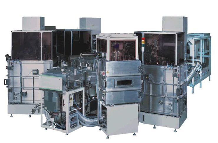
Eagle XP8 is a high productivity 300mm tool for PEALD applications. The Eagle XP8 PEALD system can be configured with up to four Dual Chamber Modules (DCM), enabling eight chambers in high volume production within a very compact footprint. (www.asm.com)

 
The award was received by ASM in recognition of its ALD technology and performance in production at TSMC fabs. During the presentation, TSMC explained three points that contributed to the award to ASM.

1) Cutting-edge tool innovations for advanced nodes.
2) Superb support to achieve quick solutions on consigned tools.
3) Great record of on-time tool delivery.

"We are very honored to receive this prestigious award from TSMC and thank TSMC for this recognition," said Chuck del Prado, CEO and President of ASM International, "ASM highly values our partnership with TSMC and we are very pleased that our Pulsar ALD and Eagle XP8 PEALD tools have provided strong benefits to TSMC in its production fabs."
TSMC is the world's largest semiconductor manufacturing foundry. TSMC hosts the Supply Chain Management forum annually to show appreciation for the support and contributions of its suppliers and to recognize outstanding equipment and materials suppliers.
 
 
ASM A412 Large Batch Furnaces form inside a TSMC 300mm Fab (Photo : Copyright® Taiwan Semiconductor Manufacturing Company Limited 2010-2016, All Rights Reserved. ) 

Sunday, February 26, 2017

Taiwan first, Korea second

Taiwan Maintains Largest Share of Global IC Wafer Fab Capacity
South Korea narrows gap with Taiwan; China  shows biggest  increase, accounts for nearly 11%

Where all those ALD tools shuffling wafers? Very few are in Europe - most of them are installed in Asia and that is Taiwan, South Korea and Japan and a considerable amount of them in USA (Fabs of Intel, Micron, Globalfoundries and Samsung) and with a growth in China as well.

IC Insights recently released its new Global Wafer Capacity 2017-2021 report that provides in-depth detail, analyses, and forecasts for IC industry capacity by wafer size, by process geometry, by region, and by product type through 2021.


Full article : LINK

Friday, February 24, 2017

Aixtron announced its financial results for fiscal year 2016

AIXTRON SE (FSE: AIXA; OTC: AIXNY), a leading provider of deposition equipment to the semiconductor industry, today announced its financial results for fiscal year 2016 and the fourth quarter 2016. 

Slide from earnings call (aixtron.com)
Following a strong second half, AIXTRON met its guidance published at the beginning of the year. At EUR 196.5 million, total revenues for 2016 virtually matched the previous year’s figure (2015: EUR 197.8m), while Q4/2016 revenues came to EUR 89.8m (Q3/2016: EUR 51.2m). This figure, which represents the highest quarterly revenues since 2011, was due to a high volume of planned system shipments. The largest contributions came from production systems for LED, telecom and optoelectronics, as well as for the silicon industry. 
Silicon that is about 21% of Aixtron´s revenue supplies the following thechnologies by ALD and CVD:
• DRAM Dielectric and Metal Electrode
• Flash Inter Poly Dielectric and Metals
• ReRAM and PCRAM Active element and Electrode
• Logic Gate stack
• Logic High MobilityChannel
The Aixtron workhorse in 300mm - the ALD multichamber technology that saw it first steps when Aixtron tool over US ALD/CVD OEM Genus mor that 10 years ago. Slide from earnings call (aixtron.com)


The following slide deck was published by Aixtron AG in conjunction with their 2016 Q4 earnings call : http://www.aixtron.com/fileadmin/user_upload/IR/2016/FY-2016/170223.1_FY_2016_IR_Master_Presentation_approved.pdf

Earnings call transcript : http://seekingalpha.com/article/4049721-aixtrons-aixg-ceo-martin-goetzeler-q4-2016-results-earnings-call-transcript?part=single

Thursday, February 23, 2017

Korean ALD OEM business is growing in OLED & Memory

According to Seeking Alpha, Korean ALD OEMs led by Jusung Engineering is growing quick for flexible OLED and Memory business (3DNAND & DRAM). It will be interesting to see if this will be verified when the Research Companies will release their 2016 numbers in the next 1-2 months. Please keep in mind that ALD is not always ALD and that Lam Research have a lot of dielectric CVD business in 3DNAND shuffling those 64 Layer stacks.

 Jusung Engineering (jseng.com)
 
Seeking Alpha summary:
  • Applied Materials is facing a two-pronged attack on its entrenched PECVD thin film deposition technology in OLED displays and memory devices from Atomic Layer Deposition (ALD) technology.
  • Korean ALD equipment suppliers Jusung Engineering and NCD are gaining market share from Applied Materials in flexible OLED displays for smartphones.
  • Korean ALD equipment suppliers Jusung and Wonik IPS and U.S. supplier Lam Research are rapidly gaining market share from Applied Materials in 3D NAND and DRAMs.
 Full article: LINK

Friday, February 17, 2017

ASM International to report operating results for the 2016 / 4Q March 2, 2017

ASM International N.V. (Euronext Amsterdam: ASM) will report operating results for the 2016 fourth quarter ended December 31, 2016 at approximately:
  • 18:00 p.m. Continental European Time - Thursday, March 2, 2017.
  • 12:00 a.m. (noon) US Eastern Time - Thursday, March 2, 2017.
ASM International will host an investor conference call and webcast on Friday, March 3, 2017 at 15:00 Continental European Time (9:00 a.m. - US Eastern Time).
The teleconference dial-in numbers are as follows: 
  • United States:         +1 212 444 0895
  • International:           +44 (0)20 3427 1913
  • The Netherlands:     +31 (0)20 716 8295
  • Access Code:          8413062
A simultaneous audio webcast and replay will be accessible at www.asm.com.


Friday, February 10, 2017

Globalfoundries announces a Global expansion

Globalfoundries announced a Global expansion today.  Investments across existing and new Fabs announced, all connected by growing customer demand.

Santa Clara, Calif., February 9, 2017 – GLOBALFOUNDRIES today announced plans to expand its global manufacturing footprint in response to growing customer demand for its comprehensive and differentiated technology portfolio. The company is investing in its existing leading-edge fabs in the United States and Germany, expanding its footprint in China with a fab in Chengdu, and adding capacity for mainstream technologies in Singapore.

 
In Germany, GF plans to build up 22FDX® 22nm FD-SOI capacity at is Fab 1 facility in Dresden to meet demand for the Internet of Things (IoT), smartphone processors, automotive electronics, and other battery-powered wirelessly connected applications, growing the overall fab capacity by 40 percent by 2020. Dresden will continue to be the center for FDX technology development. GF engineers in Dresden are already developing the company’s next-generation 12FDXTM technology, with customer product tape-outs expected to begin in the middle of 2018.


In China, GF and the Chengdu municipality have formed a partnership to build a fab in Chengdu. The partners plan to establish a 300mm fab to support the growth of the Chinese semiconductor market and to meet accelerating global customer demand for 22FDX. The fab will begin production of mainstream process technologies in 2018 and then focus on manufacturing GF’s commercially available 22FDX process technology, with volume production expected to start in 2019.

Continue:  https://t.co/R2nMYWJSa0


Thursday, February 9, 2017

Toshiba Starts Construction of Fab 6 and Memory R&D Center at Yokkaichi, Japan

Yokkaichi, Japan—Toshiba Corporation (Tokyo: 6502) today announced that it has started construction of a new state-of-the-art semiconductor fabrication facility, Fab 6, and a new R&D center, the Memory R&D Center, at Yokkaichi Operations in Mie prefecture, Japan, the company’s main memory production base. 
 

Fab 6 will be dedicated to production of BiCS FLASH™, Toshiba's innovative 3D Flash memory1. Like Fab 5, construction will take place in two phases, allowing the pace of investment to be optimized against market trends, with completion of Phase 1 scheduled for summer 2018. Toshiba will determine installed capacity and output targets and schedules by closely monitoring the market.

Toshiba will also construct a Memory R&D Center adjacent to the new fab, with completion targeting December 2017. The facility will advance development of BiCS FLASH™ and new memories. 


Toshiba is determined to enhance its competitiveness in the memory business by timely expansion of BiCS FLASH™ production in line with market trends, and to retain leadership in innovation in the memory business.

Wednesday, February 8, 2017

Intel to finish Fab 42 in Arizona & bring new 7nm capacity online

Digitimes Research: China makers aggressively expanding AMOLED capacity

Digitimes Research reports: "Seven China-based panel makers have been expanding existing or setting up new AMOLED production capacities, with total annual capacity estimated to increase from 272,000 square meters in 2016 to 1.584 million square meters in 2018, 4.464 million square meters in 2019, and 7.864 million square meters in 2020 at a 2016-2020 CAGR of 131.9%, according to Digitimes Research."
 
 
Royole’s Flexible Display : Since inception, we have dedicated ourselves to the development of innovative flexible display technologies and applications, covering novel materials, processes, circuits, manufacturing tools and others, which enabled us to demonstrate the world’s thinnest (0.01 mm) full-color flexible display with 1.00 mm bending radius. (www.royole.com)

Samsung Display and LG Display is still well in the lead now and will stay so also until 2020. However, a transition to flexible AMOLED by the South Korea based companies is ongoing (46.1% in 2016 to 72.6% in 2020).
 
2016 to 2020 AMOLED Production

South Korea: 4.945 to 15.130 million square meters
China: 272,000 to 7.864 million square meters
 
If ALD will make progress in this market the market will be very big and lead to big investments in ALD equipment and enhanced world consumption of ALD precursors like TMA.
 
Chinese display companies mentioned in the report: BOE Technology, Tianma Micro-electronics, Visionox, EverDisplay Optronics, China Star Optoelectronics Technology, Truly Opto-Electronics and Royole

Thursday, February 2, 2017

Veeco Enters into Agreement to Acquire Ultratech


Ultratech, Inc.
Feb 2, 2017

PLAINVIEW, NY and SAN JOSE, CA -- (Marketwired) -- 02/02/17 --
  • Creates a leading equipment supplier to the growing Advanced Packaging industry
  • Increases scale and revenue diversification to improve profitability through industry cycles
  • Transaction valued at approximately $815 million, expected to be immediately accretive to non-GAAP EPS
  • Conference Call at 5:00pm ET today
Veeco Instruments Inc. (NASDAQ: VECO), a global leader of advanced thin film etch and deposition process equipment, and Ultratech, Inc. (NASDAQ: UTEK), a leading supplier of lithography, laser-processing and inspection systems used to manufacture semiconductor devices and LEDs, today announced that they have signed a definitive agreement for Veeco Instruments Inc. ("Veeco") to acquire Ultratech, Inc. ("Ultratech"). The Boards of Directors of both Veeco and Ultratech have unanimously approved the transaction.


ALD is not reported by neither conmpany. One can assume however that ALD is big part of the sector "Scientiffic" ta Ultratech. According to Gartener Ultratech had almost USD 9M in reveue 2015 From the Investor slides given here : LINK

Ultratech shareholders will receive (i) $21.75 per share in cash and (ii) 0.2675 of a share of Veeco common stock for each Ultratech common share outstanding. Based on Veeco's closing stock price on February 1, 2017, the transaction consideration is valued at approximately $28.64 per Ultratech share. The implied total transaction value is approximately $815 million and the implied enterprise value is approximately $550 million, net of Ultratech's net cash balance as of December 31, 2016. Post transaction it is projected that Ultratech shareholders will own approximately 15 percent of the combined company.

Ultratech is a recognized leader of lithography products for Advanced Packaging applications and for LEDs and is a pioneer for laser spike anneal technology used for the production of semiconductor devices. In addition, the company offers wafer inspection solutions leveraging its proprietary coherent gradient sensing (CGS) technology which address a wide variety of semiconductor applications.

"The strategic combination will establish Veeco as a leading equipment supplier in the high growth Advanced Packaging industry. Ultratech's leadership in lithography together with Veeco's Precision Surface Processing (PSP) solutions form a strong technology portfolio to address the most critical Advanced Packaging applications. We believe our complementary end market exposure and customer relationships will create the ideal platform to accelerate growth," said John R. Peeler, Veeco's Chairman and Chief Executive Officer. "Ultratech is a great fit with our strategy to profitably grow our business and diversify our revenue. We expect this transaction to be immediately accretive to adjusted EBITDA and non-GAAP EPS."

Ultratech Chairman and Chief Executive Officer, Arthur W. Zafiropoulo said, "Both companies have a strong heritage of developing innovative and cutting-edge technologies. The combined company will create a formidable team to execute against growth opportunities and deliver significant value to customers and shareholders."

Veeco expects to realize approximately $15 million in annualized run rate synergies within 24 months after closing, to be achieved through increased efficiencies and leveraging the scale of the combined businesses. The combined company is expected to have an efficient balance sheet, benefiting from the deployment of excess cash.
0
The transaction is expected to close in the second calendar quarter of 2017, subject to approval by Ultratech shareholders, regulatory approvals in the U.S. and other customary closing conditions.

Monday, January 30, 2017

Hitachi High-Technologies and Picosun Oy launch a collaboration in Plasma-enhanced ALD

Tokyo, Japan and Espoo, Finland - 30 January 2017 - Hitachi High-Technologies Corporation (TSE:8036, Hitachi High-Tech) and Picosun Oy announce a revolutionary technological co-operation in plasma-enhanced atomic layer deposition (PE-ALD). The aim of this co-operation is to bring thin film coating technologies to a completely new level. Hitachi High-Tech’s and Picosun’s joint breakthrough, the novel Microwave Electron Cyclotron Resonance (ECR) ALD technology will disrupt all advanced semiconductor industries. 

Promotion Video: MECRALD - novel, revolutionary plasma-enhanced ALD technology By Hitachi High-Technologies and Picosun. (youtube.com)

In the PE-ALD reactor, Hitachi High-Tech’s powerful ECR plasma generator is integrated with Picosun’s industry-proven, digitally controlled ALD system. Consequently, the quality of the deposited materials is substantially better, and the deposition process is much more precise than existing traditional ALD and plasma-enhanced ALD methods.

Some superior results for various nitride and oxide films have been confirmed with 300 mm semiconductor wafers so far and some other process applications are under evaluation.

About Hitachi High-Technologies Corporation

Hitachi High-Technologies Corporation, headquartered in Tokyo, Japan, is engaged in activities in a broad range of fields, including Science & Medical Systems, Electronic Device Systems, Industrial Systems, and Advanced Industrial Products. The company's consolidated sales for FY 2015 were approx. 629 billion [USD5.8 billion]. For further information, visit http://www.hitachi-hightech.com/global/.

About Picosun Oy

Picosun provides the most advanced ALD thin film coating technology to enable the industrial leap into the future, with turn-key production solutions and unmatched expertise in the field. Today, PICOSUN™ ALD equipment are in daily manufacturing use in numerous major industries around the world. Picosun is based in Finland, with subsidiaries in North America, Singapore, Taiwan, China, and Japan, and a world-wide sales and support network. For more information visit www.picosun.com. 

Wednesday, January 25, 2017

Lam Research doubled install base of ALE in Logic 2016

Lam Research just presented their 4Q/2016 earnings. 2016 was the fifth consecutive year of growth and outperformance for Lam with a shipments CAGR of almost 20% over that period and shipments grew to a record $6.7 billion. As an example of the success 3D NAND shipments grew by over 80% in 2016, almost twice the rate of growth in NAND’s WFE. Please find all detailas in the Seeking Alpha Earings Call Transcript here

With respect to new existing atomic level control technology Lam has strengthened its momentum in foundry and logic with significant application share gains from the 2016 nodes to the 10 and 7 nanometer nodes. As an example, during the quarter they more than doubled their install base for  Atomic Layer Etch (ALE) system for logic self-aligned contact application with their dielectric etch product and mixed mode pulsing technology.

Seeking Alpha Earings Lam Research Call Slides here.

Wednesday, January 18, 2017

Encapsulix SAS selected as supplier of ALD-TFE deposition systems by leading Asian AMOLED manufacturer

January 16, 2017 : Encapsulix SAS today announced that it has been selected as the supplier of ALD-TFE deposition systems by a leading Asian AMOLED manufacturer. The first tool is presently under construction and scheduled for operation from the spring of 2017 onwards. The systems will be used to encapsulate flexible AMOLED displays with multifunctional nanolaminated coatings. The order was awarded to Encapsulix SAS after an extensive evaluation of available ALD equipment suppliers of barrier and encapsulation coatings.

The Infinity ALD equipment platform has the unique capability to deposit the most advanced nano-engineered coatings in a manufacturing environment. These coating have an overall thickness in the 20-50nm range, and typically comprise tens of sublayers of up to 10 different materials with thicknesses in the nanometer range. A wide range of available materials includes both inorganic (e.g. Al2O3, SiO2, ZrO2, TiO2, SiNx, HfO2,..) and organic (Alucone, Zircone, ..) nanolayers allowing to engineer the barrier, mechanical, optical en electrical properties at the atomic scale.

« This order confirms the technological superiority and leading Cost-Of-Ownership of our ALD-TFE equipment and process solutions for AMOLED manufacturing » stated Dr. Jacques Kools, founder and CEO of Encapsulix SAS. He also stated « We are now seeing rapid market adaptation of Nanolaminated ALD-TFE as the ideal solution for the emerging application of foldable OLED devices. »

About Encapsulix, Encapsulix was founded to address the geometric scaling of critical deposition requirements for industrial & microelectronic devices and foils. The company has its development and headquarters in Simiane- Collongue France, equipment development, sales and service in the USA. 
For more information:
Contact: www.encapsulix.com

For those of you attending ALD For Industry in Dresden 17-18 of January you will have an excellent opportunity to listen and be enlightened by Dr. Kools himself giving a talk entitled "Industrial deployment of nano-engineered ultrabarriers for encapsulation of organic electronic".

Friday, January 6, 2017

Samsung Electronics forecasts fourth-quarter profit at over three-year high

REUTERS : Samsung Electronics Co Ltd  said on Friday its fourth-quarter profit likely leapt 50 percent from a year earlier to its highest level in more than three years, beating expectations on strong chip sales and a smartphone rebound.


 The upbeat outlook comes despite a slight fall in revenue and the anticipated $2.1 billion profit hit from the withdrawal of the fire-prone Galaxy Note 7 premium smartphone in October.

The guidance points to a more rapid recovery for the mobile business than many analysts had anticipated after one of the biggest product safety failures in tech history, and reflects steady price increases for memory chips.

"Samsung posted solid earnings only with sales of older smartphone models like the S7 after the Note 7's discontinuation," said Kim Sung-soo, a fund manager at LS Asset Management.

"This makes me have hopes for the (Galaxy) S8. Should they fare well, I expect Samsung to report record earnings this year."

The world's biggest maker smartphones, TVs and memory chips will not disclose detailed earnings, including the performance of its individual businesses, until late January.

Analysts expect Samsung's chip division to earn a record of more than 4 trillion won in operating profit in October-December thanks to strong demand from smartphone makers, including major client Apple Inc, and high-end data storage products.

More: Samsung expects a rise in profit thanks to chips and OLED

The Korean conglomerate's mobile division also bounced back after Note 7's fiery death.

According to the Korean chaebol's earnings forecast for October to December last year, its operating income for the fourth quarter was 9.2 trillion won ($7.8 billion). That's 50 percent larger than the income posted for the same period in 2015 and the highest since the third quarter of 2013, thanks mostly to its its strong chip and OLED sales.

The company’s display division probably posted a profit of 1.1 trillion won. The proliferation of OLED screens should help in coming quarters: Apple is said to be planning to adopt the technology in at least one new iPhone later this year.[Bloomberg]

Thursday, January 5, 2017

Gartner Forecasts Flat Worldwide Device Shipments Until 2018

Emerging Devices Can Enhance Conventional Device Sales

Worldwide combined shipments of PCs, tablets, ultramobiles and mobile phones are projected to remain flat in 2017, according to Gartner, Inc. Worldwide shipments for these devices are projected to total 2.3 billion in 2017, the same as 2016 estimates.
 
Full report : LINK


Thursday, December 22, 2016

SK Hynix to invest $2.7 billion on memory chip output as demand soars

According to Reuters the world´s number two memory maker from South Korea - SK Hynix Inc - said it will invest 3.16 trillion won ($2.7 billion) in its home country and China to boost memory chip production, seeking to capitalize on an industry-wide surge in demand.

 Most of the investment will be for a new Fab for 3DNAND flash chips used in non-volatile data storage in Smartphones, Tablets and Laptop Flash SSD hard drives.
 
The rivals Samsung and Toshiba Corp has also announced spending on new Fabs memory chip production.
 
REUTERS article : LINK

Applied Materials reportedly missing out on ALD for OLED encapsulation

Applied Materials is world leading in CVD processing for wafer and display. However, i big part of the CVD equipment market today is the booming segment of ALD where Applied only have single digit percentage of the revenue. According to a recent report by Seeking Alpha, "Applied Materials is facing strong competition as its deposition technology is being supplanted by Atomic Layer Deposition at Samsung Electronics and LG Display". Other applications where Applied Materials did not enter with ALD include:
  • DRAM High-k MIM Capacitors
  • Logic High-k Metal Gate Stack 
  • Double Patterning 
However, Applied Materials has reported strong revenue in Selective Etch and Olympa ALD (>USD 230M) Possibly they have some advanced Spatial ALD technology up the sleeve also for OLED encapsulation.

 Watch For Big Display Equipment Cancellations Coming From Applied Materials

  • Tight supply of a critical piece of OLED equipment from Canon Tokki will limit OLED production in 2017 and impact Applied Material's sales of supplemental equipment.
  • Applied Materials also is facing strong competition as its deposition technology is being supplanted by Atomic Layer Deposition at Samsung Electronics and LG Display.
  • As much as $1 billion in display equipment from Applied Materials could be cancelled in 2017.
Full report

More details on the Canone Tokki and Apple OLED roll out story here from Bloomberg:

Apple's Search for Better iPhone Screens Leads to Japan's Rice Fields [Bloomberg TV]

The ELVESS OLED mass production system. Source: Canon Tokki Corp.

Wednesday, December 21, 2016

CVD Acquires Assets of Danish Tantaline A/S

CENTRAL ISLIP, N.Y., (Business Wire) – December 19, 2016 - CVD Equipment Corporation (NASDAQ: CVV), a leading provider of chemical vapor deposition systems, has purchased certain assets (including all of the IP) formerly owned by Tantaline A/S of Nordborg, Denmark through our wholly owned subsidiary, CVD Materials Corporation. Formed in 2007, as a spin off from The Danfoss Group, Tantaline A/S established itself as a leader in the commercialization of tantalum treated parts for corrosion resistance. We have now established in Nordborg a new and wholly owned CVD subsidiary operating under the name Tantaline CVD ApS (“Tantaline®”). 

 This innovative tantalum chemical vapor technology, called Tantaline® treatment, is used to create a tantalum surface alloy on parts including valves, fittings, autoclaves, process chambers, flow reactors, fasteners, mixers, flowmeters, and medical devices, as well as other parts that are prone to corrosion in harsh environments. These parts are used across a broad range of industries including chemical processing, oil & gas, mining, pharmaceutical, and medical. In hot corrosive acidic environments (>150°C) such as sulfuric, nitric, and hydrochloric acids, Tantaline® treated parts outperform most high priced specialty alloys and perform nearly at the level of solid tantalum parts. Tantaline® treatment therefore provides solid tantalum like superior corrosion resistance at a lower part cost.

ALD and 300 mm Wafer processing - Fabs, Applications & OEMs

IC Insight has released a number of reports now in December (see links below). One of them is the new Global Wafer Capacity 2017-2021 and here it is clear - when it comes to high volume production and wafer size it is clear that 450mm is dead - nobody is going down that path. For the top ALD OEMs the main revenue is on 300mm wafer processing tools, single wafer, multi wafer and large batch furnaces.

Since Samsung went ahead with high volume manufacturing using an ALD High-k as node dielectric at 90 nm for DRAM MIS Capacitors ALD has mainly been employed on 300 mm wafers. I am guesstimating that 80 to 90 % of the total annual revenue for ALD equipment are 300 mm wafer processing equipment. The top suppliers in annual revenue for the 300 mm market in descending order according to my estimates for 2015 was: 

1. ASM International
2. Tokyo Electron
3. Kokusai
4. Lam Research
5. Jusung Engineering
6. Wonik IPS
7. Aixtron
8. Applied Materials
9. Picosun
10. Ultratech. 

Adding to that there are a number of OEMs in South Korea besides Jusung and Wonik IPS that are supplying 300 mm ALD tools but I lack insight into them and therefore I am rather leaving them outside the list. By the end of the 1st quarter 2017 there will be new numbers available for a estimation for 2016 and it will be interesting to see if Applied Materials and Lam Research have taken market shares in ALD for the booming 3DNAND, patterning business and maybe BEOL applications where ASM is not that strong and Large Batch Furnaces are more seldom used (TEL & Kokusai).

Following the table below from IC Insight you can see that  the top 10 manufacturers having 300 mm fabs and thats´s where you will find a majority of those ALD reactors shuffling 300 mm wafers for the major ALD process modules that are:

  • DRAM Capacitors
  • HKMG Transistor stacks
  • Liners & Spacers
  • Multipple patterning
  • 3DNAND Gate stacks
  • Cu seed, barries and caps inBEOL interconnects
Most interestingly the memory companies (Samsung, Micron & SK Hynix) are shuffling the most amount of 300 mm wafers, almost 50% of them, and besides the big ALD install base in Logic Gate stacks and patterning you will find a huge amount of installed ALD tools in those DRAM and NAND flash fabs. 


Total Memory Market Forecast to Increase 10% in 2017
-- December 20, 2016
Number of IC Manufacturers Using 300mm Wafers Less than Half Using 200mm Wafers-- December 16, 2016
Five Suppliers Hold 41% of Global Semiconductor Marketshare in 2016-- December 06, 2016

Tuesday, December 20, 2016

Jusung Engineering signs USD 15 million contract with Chinese Kunshan OLED Line


Jusung Engineering Says it has signed a 18.03 billion won (US$15.2 million) contract with Chinese Kunshan Govisionox Optoelectronics Co., Ltd. to provide display manufacturing equipment. (Source : LINK)

According to Iter News the equi9pment from Jusung is for OLED Encapsulation and the OLED Display ilne in Kushan will come online 4Q 2017 and will have a monthy capacity of 8,000 sheets. Reportedly, Jusung have previously supllied equipment also fro LG Display and Innolux in Taiwan.

Jusung´s platform for OLED Encapsulation with a new concept for zero-damage plasma technolog producing a very high-quality thin film  technology at low temperature (www.jseng.com)

According to Jusung website they supply the following technology for OLED Display encapsulation:

KEY BENEFITS
CVD/ALD two-way encapsulation system suitable for large-area encapsulation
- Large-area encapsulation using new concept plasma technology for the first time in the world TSD-CVD/ALD (Time Space Divided)

KEY APPLICATIONS
- Encapsulation (SiO / SiOX / SiN / Al2O3)
- Barrier (SiO / SiOX / SiN / Al2O3) 

Thursday, December 15, 2016

Samsung Likely to Spin off Foundry Business Division

SEOUL,KOREA, 12 December 2016: Samsung Electronics is considering a reorganization of the System LSI division in order to systematically grow the system semiconductor business. The company is planning to separate the design and manufacturing sectors in the business unit and divide or spin off it to fabless and foundry business divisions

Wednesday, December 14, 2016

SEMI Forecasts - 62 New Fabs to Start Operation 2017 to 2020

Driving the growth in ALD Equipment 2017 to 2020 will be the building and starting of operations of 38 Front End Fabs for Foundry (20), Logic (5) and Memory (13). For this CVD, ALD and Advanced Etch Equipment, Including ALE will be needed for HVM of sub 20 nm nodes Logic & DRAM and next Generation 3DNAND.

SEMI Reports: Data from SEMI’s recently updated World Fab Forecast report reveal that 62 new Front End facilities will begin operation between 2017 and 2020. This includes facilities and lines ranging from R&D to high volume fabs, which begin operation before high volume ramp commences. Most of these newly operating facilities will be volume fabs; only 7 are R&Ds or Pilot facilities.


SEMI's latest World Fab Forecast. By product type, 32 percent are foundries, 21 percent are Memory, 11 percent LED, then Power, MEMS, Logic, Analog, and Opto, in decreasing order. Between 2017 and 2020, China will see 26 facilities and lines beginning operation, about 42 percent of the worldwide total currently tracked by SEMI.  The majority of the facilities starting operation in 2018 are Chinese-owned companies. The peak for China in 2018 comes mainly from foundry facilities (54 percent). The Americas region follows with 10 facilities, and Taiwan with 9 facilities. Data: SEMI.
 

New facilities & lines starting operation by product type from 2017 to 2020. Data: SEMI.

Tuesday, December 13, 2016

Semiconductor Equipment Sales Forecast ─ $40 Billion

TOKYO — December 13, 2016 — SEMI, the global industry association representing more than 2,000 companies in the electronics manufacturing supply chain, today reported that worldwide sales of new semiconductor manufacturing equipment are projected to increase 8.7 percent to $39.7 billion in 2016, according to the SEMI Year-end Forecast, released today at the annual SEMICON Japan exposition. In 2017, another 9.3 percent growth is expected, resulting in a global semiconductor equipment market totaling $43.4 billion.
The SEMI Year-end Forecast predicts that wafer processing equipment, the largest product segment by dollar value, is anticipated to increase 8.2 percent in 2016 to total $31.2 billion. The assembly and packaging equipment segment is projected to grow by 14.6 percent to $2.9 billion in 2016 while semiconductor test equipment is forecast to increase by 16.0 percent, to a total of $3.9 billion this year. For 2016, Taiwan and South Korea are projected to remain the largest spending regions, with China joining the top three for the first time. Rest of World (essentially Southeast Asia), will lead in growth with 87.7 percent, followed by China at 36.6 percent and Taiwan at 16.8 percent. SEMI forecasts that in 2017, equipment sales in Europe will climb the most, 51.7 percent, to a total of $2.8 billion, following a 10.0 percent contraction in 2016. In 2017, Taiwan, Korea and China are forecast to remain the top three markets, with Taiwan maintaining the top spot even with a 9.2 percent decline to total $10.2 billion. Equipment sales to Korea are forecast at $9.7 billion, while equipment sales to China are expected to reach $7.0 billion. The following results are given in terms of market size in billions of U.S. dollars:

Monday, December 12, 2016

Flexible displays to grow 135% in 2017 and are expected to reach 139 million units

IHS Markit reports: As more smartphone manufacturers build designs using flexible display technology, shipments of flexible displays are expected to reach 139 million units in 2017, an increase of 135 percent compared to 2016. Further, the flexible displays are expected to comprise 3.8 percent of total display unit shipments in 2017.
  • Vivo and Xiaomi launched their first smartphones with flexible active-matrix organic light-emitting diode (AMOLED) displays in 2016.
  • Apple is expected to launch its new iPhone using flexible AMOLED display in 2017.
  • In 2017 Samsung Display and LG Display will start operating new fabs for flexible displays.
 Flexible display shipment forcast (Source IHS Markit)

Friday, December 9, 2016

Aixtron considers partial sell-off after Chinese deal blocked

REUTERS : German semiconductor chipmaking machinery company Aixtron (AIXGn.DE) may sell off part of its business, its chief executive said in an interview published on Friday, opening the door for bidders after a deal with a Chinese company collapsed.

China's Fujian Grand Chip Investment Fund dropped its 670 million-euro ($712 million) bid for Aixtron earlier this week after the United States blocked the deal on security grounds, throwing the German company's future into doubt.


Martin Goetzeler, Chief Executive Officer (Aixtron.com)
 
"There are two options: First, we could hope that the markets for our products recover and continue investing high sums in new equipment. But that would come with high development and ramp-up costs, and risks," Martin Goetzeler told German daily Handelsblatt.

"Or Aixtron could shrink, divest technologies and continue with a specialized offering," he said.


Aixtron makes devices which produce crystalline layers from gallium nitride that are used as semiconductors in weapons systems.

Its technology is being used to upgrade U.S. and foreign-owned Patriot missile defense systems and the U.S. Treasury said the deal had been blocked due to national security risks.

Full report at Reuters : LINK

Thursday, December 8, 2016

China's Fujian drops Aixtron bid after U.S. blocks deal

Seeking Alpha reports:
  • China's Fujian Grand Chip Investment Fund drops its takeover bid for German chip equipment maker Aixtron (NASDAQ:AIXG), saying its offer had lapsed as it had failed to obtain U.S. regulatory approval for the deal.
  • AIXG's technology is being used to upgrade both U.S. and foreign-owned Patriot missile defense systems, and the U.S. blocked the deal last Friday due to national security risks.

Taiwan's TSMC to build $16bn advanced chip facility

Sunday, December 4, 2016

Aixtron, Fujian to explore what is left of deal after U.S. veto

(REUTERS): German semiconductor equipment maker Aixtron will explore with its Chinese suitor what can be salvaged of the planned takeover after a U.S. presidential order ruled the deal posed a national security risk, the company said on Saturday.

U.S. President Barack Obama blocked China's Fujian Grand Chip Investment Fund (FGC) from acquiring Aixtron's U.S. business, the Treasury Department said on Friday.


"The bidder and Aixtron are evaluating the impact of the Order on the conditions to be fulfilled under the takeover offer and will coordinate with the German Federal Financial Supervisory Authority (BaFin) to examine the consequences of the Order on the takeover process," Aixtron said in a statement.

It added the presidential order was limited to Aixtron's U.S. business and did not per se prohibit the acquisition of Aixtron shares and American depositary shares FGC.

Aixtron has previously said that scrapping the proposed deal would mean it would have to cut costs and jobs would be at risk. 

It added the presidential order was limited to Aixtron's U.S. business and did not per se prohibit the acquisition of Aixtron shares and American depositary shares FGC. Aixtron has previously said that scrapping the proposed deal would mean it would have to cut costs and jobs would be at risk.

Saturday, December 3, 2016

Versum Materials Reports Strong Fourth Quarter

TEMPE, Ariz.–(BUSINESS WIRE)–Dec. 1, 2016– Versum Materials, Inc. (NYSE: VSM), a leading materials and equipment supplier to the semiconductor industry, today reported results for the fourth quarter and full fiscal year ended September 30, 2016. Net income for the fourth quarter of $45 million was up 5% versus the comparable prior year period while fiscal 2016 net income of $212 million was up 15% versus prior year. Adjusted EBITDA for the quarter of $78 million was up 12% versus the comparable prior year period while fiscal 2016 adjusted EBITDA of $327 million was up 8% versus prior year.

The results reflect the performance of Versum Materials as a wholly owned subsidiary of Air Products and Chemicals, Inc. (NYSE: APD) (“Air Products”), and are derived from the consolidated financial statements and accounting records of Air Products as if Versum operated on a stand-alone basis during the periods presented and were prepared in accordance with GAAP.

“For the Versum team, this fourth quarter closes a strong final chapter as a subsidiary of Air Products and sets us up for a bright future ahead as an independent company, focused on delivering meaningful value to our customers, shareholders and employees,” said Guillermo Novo, our President and Chief Executive Officer. “With a broad portfolio of products and services, Versum is uniquely positioned to grow and lead through innovative solutions and services for our customers in the semiconductor industry.”
Full report : LINK

President Obama set to block Aixtron sale

Seeking Alpha reports that President Obama is poised to block a Chinese company from buying Germany's Aixtron (NASDAQ:AIXG) because Northrop Grumman (NYSE:NOC), a major U.S. defense contractor, is among the chip equipment maker's customers.

It would mark only the third time in more than a quarter century that the White House rejected an investment by an overseas buyer as a national security risk.

Aixtron shares -6.5% in Frankfurt.


China Warns U.S. Against Blocking Aixtron Takeover

Aixtron shares fall amid U.S. national security concerns over acquisition by China’s Fujian Grand Chip Investment Fund [Wall Street Journal]

Obama bars China's Fujian from buying Aixtron's US business


The headquarters of German chip equipment maker Aixtron SE is pictured ... The Treasury Department said Obama was blocking the deal .. [Reuters]

Warum redet Amerika in der Aixtron-Ăœbernahme mit?

Die Ăœbernahme des deutschen Maschinenbauers Aixtron durch einen chinesischen Investor ruft die groĂŸe Politik in Washi [FAZ - Frankfurter Allgemeine Zeitung]

Friday, November 18, 2016

Applied Materials reports strong revenue in Selective Etch and Olympa ALD (>USD 230M)

Applied Materials Inc, the world’s largest supplier of tools used to make semiconductors, reported lower-than-expected quarterly revenue, largely due to slowing smartphone sales. However, it seems that they had recent success in selective etch and Olympia ALD sales.


Applied Materials' CEO Gary Dickerson reported the following on Q4 2016 Results: "Our leadership businesses are in a really great position to grow. In 2016, we converted well over 90% of our development positions to volume production wins. We’re also making significant market share gains in Etch and CVD. Fiscal 2016 was our third consecutive year of growth in CVD and fourth consecutive year of growth in Etch where revenues reached a 9-year high. Overall our combined Etch and CVD revenues exceeded $2.7 billion for the year. I’m very excited by our product pipeline line in Etch and ALD. We’re seeing rapid adoption of our innovative new solutions, including selective Etch and Olympia ALD that together generated more than $230 million of revenue this year."

Source: Applied Materials' (AMAT) CEO Gary Dickerson on Q4 2016 Results - Earnings Call Transcript by Seeking Alpha.


Wednesday, November 16, 2016

Aixtron returns to positive free cash flow in Q3, boosted by sales of AIX R6 system inventory

Semiconductor Today reports: The majority of AIX R6 MOCVD system inventory (for GaN LEDs) – which amounted to €19.3m at the end of September – was sold in Q3 (and will be shipped in the coming months). Also, throughout Q3 there were strong shipments of Planetary reactor systems particularly for red, orange, yellow (ROY) LED optoelectronics and power electronics. "We continue to be in a solid position in MOCVD outside GaN LEDs," notes president & CEO Martin Goetzeler. Also, Aixtron has completed one customer's qualification program for atomic layer deposition (ALD) tools for high-k oxide films; in Q3/2016 such silicon applications (including spares) comprised 25% of total revenue. 

Full story: LINK


Tuesday, November 15, 2016

Germany’s Merck Q3 profit, sales soar on Sigma-Aldrich acquisition

ICIS Reports : Merck posted a 19.3% year-on-year increase in third-quarter sales at €3.7bn and a post-tax profit of €460m, up 25.9%, benefitting from its $17bn acquisition of US’ Sigma-Aldrich in 2015, the German chemical major said on Tuesday.

Merck’s Performance Materials division, however, posted a 1.3% fall in third-quarter sales year on year to €645m, while earnings before interest, taxes, depreciation and amortisation (EBITDA) pre exceptional items fell 5.4% during the period, year on year, to €282m.

“However, the acquisition-related sales increase of 3.5% attributable to the SAFC Hitech business of Sigma-Aldrich, which has been integrated into the Performance Materials business sector, had a positive impact.”

Full story : LINK

Tuesday, November 8, 2016

Aixtron announce High-k ALD customer for memory in 3Q/2016 Earnings call

AIXTRON Aktiengesellschaft's (AIXG) CEO Martin Goetzeler on Q3 2016 Results - Aixtron announce new customer in Memory in their silicon business unit (mainly ALD from ex-Genus) as The customer has qualified ALD tools for high-k oxide. In Q3 2016 silicon including spares contributed 25% of Aixtron total revenues.


Please find the full transcript of the Q3 earnings call here and the slides here. Boot supplied by Seeking Alpha.

Thursday, November 3, 2016

Details on the Veeco ALD cost reduction program from Q3 2016 Results - Earnings Call

Veeco Instruments Inc. announced September 2013 that it has signed an agreement to acquire privately held Synos Technology, Inc. (“Synos”) and went through with the acquisition. At the time Synos was developing and manufacturing Fast Array Scanning™ Atomic Layer Deposition (FAST-ALD™) systems that are enabling the production of flexible organic light-emitting diode (OLED) displays for mobile devices. 

Despite recent rumors that the display industry is adopting ALD OLED barrier technology Veeco has announced a cost savings program for ALD. Here are some insights to the Veeco ALD cost reduction program as reported during the Veeco Instruments Q3 2016 Results - Earnings Call (Seeking Alpha Transcript)


John R. Peeler - CEO, Veeco Instruments, Inc.
"More recently, we reduced investments in our atomic layer deposition technology development. We weighed the investments necessary to establish and grow a position in ALD with the potential and expected timing for returns and although we continue to make progress in our development efforts for advanced semiconductor applications, the timing for potential revenue realization was delayed. As a result, we decided to significantly reduce our ALD expenses. In total, we now expect to lower the company's cost structure by $30 million on an annual basis. These savings translate into an EBITDA break-even level at or below $75 million in quarterly revenue, starting in Q1 2017."

Shubham Maheshwari - CFO, Veeco Instruments, Inc. gave the following explanations:
  • The competitive technologies solved their problems leaving no investment for now in ALD meaning that the near-term opportunity for ALD has been pushed out and that is the reason for the ALD cost reduction program.
  • The ALD cost reduction is about $10 million of the total cost reduction program reported.
  • The spending up until now for ALD has been somewhere around low teens on an annual basis
  • Veeco will still be investing in ALD, but at a much lower amount.