Thursday, July 27, 2017

Memory chip boom - Samsung Q2 operating profit up 73 percent

Samsung Electronics said a memory chip boom that propelled it to record profit in the second quarter is likely to continue in the third, just as revenue is widely expected to benefit from sales of OLED screens to Apple.

The world’s biggest maker of memory chips, smartphones and TVs is set to smash its annual profit record after better-than-forecast performance in its mobile business lifted April-June profit slightly above its early-July guidance, analysts said.

“Looking ahead to the third quarter, the company expects favorable semiconductor conditions to continue,” Samsung said in a statement on Thursday. “Although overall earnings may slightly decline quarter-on-quarter as earnings weaken for the display panel and mobile businesses.”

Source: VentureBeat LINK

Flexible AMOLED capacity to almost double each year until 2020

OLED-Info reports that estimates by IHS that flexible AMOLED production capacity is set to increase from 1.5 million square meters to 20.1 million square meters between 2016 and 2020, which would correspond to a compound annual growth rate of 91%.

Source: OLED-Info (LINK)


The Korean CVD & ALD OEMs stocks are travelling upwards since April 2017 (see below). Surely based on investments by Samsung and SK Hynix for Foundry, DRAM and 3D-NAND but this must also reflect order intake from Korean and Chinese AMOLED 6 Gen lines to some extent.

Recent announcments for Semi orders:

Tes signed 16.75 billion won contract with Samsung Electronics Co Ltd, to provide semiconductor manufacturing system (LINK

Eugene Technology signed a 7.36 billion won contract with SK hynix to provide semiconductor manufacturing equipments (LINK)

Tes signed a 2.8 billion won contract with SK hynix Inc to provide semiconductor manufacturing equipment . (LINK)


Tuesday, July 25, 2017

Micron at Flash Memory Summit 2017

BOISE, Idaho, July 25, 2017 (GLOBE NEWSWIRE) -- Micron Technology, Inc. (NASDAQ:MU) invites you to join industry thought leaders and executives to hear strategic updates from the company on 3D NAND and NVMe technologies at the 2017 Flash Memory Summit, August 8-10, 2017, in Santa Clara, Calif. A premier sponsor, Micron is a global leader delivering solutions for the world's toughest computing and storage challenges.Micron Keynote Address - New Silicon Breakthroughs Help Next Generation Datacenters Meet Key ...

Source: Benzinga  LINK

ASM report strong order intake in ALD for 3D-NAND and Foundry in its 2Q 2017 report

For 2017, the leading ALD equipment manufacturer ASM International expect a clear improvement in the single wafer ALD market and they forecast the single wafer ALD market to reach a size of about USD 1.5 billion by 2020-2021. As a comparasion the ALD market as a whole was estimated to USD 1.4 to 1.5 billion in 2016 (Gartner, VLSI Research, TECHCET), including all segments (e.g. Semi, MEMS, PV, OLED and R&D).

ASM International N.V. (Euronext Amsterdam: ASM) today reports its second quarter 2017 operating results (unaudited) in accordance with IFRS. (LINK)

Investor presentation Q2 2017
  • New orders at €206 million were 1% above the Q1 2017 level and 29% above last year's Q2 level.
  • Net sales for the second quarter 2017 were €202 million, an increase of 40% compared to the previous quarter. Year-on-year net sales increased with 46%.
  • Net earnings of €132 million in the second quarter included a result of €84 million from the 5% sale and dilution of the ASMPT stake.
  • Normalized net earnings for the second quarter 2017 increased by €14 million compared to the first quarter 2017. Operating result increased to €38 million. The financing result included €11 million negative effects from currencies compared to €7 million negative effects in the first quarter. The result from investments decreased with €4 million due to the dilution of our stake in ASMPT. Moreover the ASMPT results in the first quarter included a one-off non-cash gain of €10 million related to the revaluation of the convertible bond.


Commenting on the results, Chuck del Prado, President and Chief Executive Officer of ASM International said: 

"In Q2 we realized sales of €202 million, which was slightly above our guidance and at a historical high quarterly level. The order intake for Q2, at €206 million, came in at the high end of the forecast and was also at the highest level in the company's history. Order intake in ALD was primarily strong from the 3D-NAND and Foundry segments. We also received several Intrepid Epitaxy orders in Q2."


OUTLOOK
Based on our current assessment, we continue to expect a clear year-on-year improvement in the single wafer ALD market in 2017, with demand in the Logic/Foundry segment remaining healthy and a strong increase in the 3D-NAND segment.

For Q3 we expect a sales level of €170-190 million, on a currency comparable level, while for the second half of 2017 as a whole we expect a sales level higher than in the first half of 2017. After the very strong orders in the past two quarters we expect order intake in Q3 at a still healthy level of €150-170 million, on a currency comparable level.

Monday, July 24, 2017

Apple to setup a 2.5-Gen OLED R&D production line in Taiwan

According to OLED-Info referring to reports from Korea, Apple ordered a 2.5-Gen OLED evaporation (CVD) equipment from Sunic System in order to build an OLED pilot line in Taiwan. The report suggests that Apple wants to develop in-house OLED technologies which will allow it to reduce its reliance on Samsung Display.


Norwegian CrayoNano Selects Veeco MOCVD System for Nanowire on Graphene Development

PLAINVIEW, NY -- (Marketwired) -- 07/24/17 -- Veeco Instruments Inc. (NASDAQ: VECO) announced today that CrayoNano AS, research leader for ultraviolet short wavelength light emitting diodes (UV-C LEDs), has ordered the Propel® Power Gallium Nitride (GaN) Metal Organic Chemical Vapor Deposition (MOCVD) System. CrayoNano will use the system to grow semiconductor nanowires on graphene for water disinfection, air purification, food processing and life science applications. 
 
 
UV-C LEDs are free of harmful mercury compared to typically 20-200 milligrams of mercury found in traditional UV lamps used in these applications. They also require minimal energy to operate and have longer life cycles compared to other purification and disinfection lighting methods. The value of the global market for UV-C LEDs used in sterilization and purification equipment is growing at a CAGR of 56% from US$28 million in 2016 to US$257 million in 2021, according to the 2016~2021 UV LED and IR LED Application Market Report by LEDinside, a division of TrendForce.

Saturday, July 22, 2017

Veeco CNT ships its 500th ALD system

As reported by Solid State Technology: Veeco Instruments (Veeco) recently announced that Veeco CNT—formerly known as Ultratech/Cambridge Nanotech—shipped its 500th Atomic Layer Deposition (ALD) system to the North Carolina State University. The Veeco CNT Fiji G2 ALD system will enable the University to perform research for next-generation electronic devices including wearables and sensors. Veeco announced the overall acquisition of Ultratech on May 26 of this year. Executive technologists from Veeco discussed the evolution of ALD technology with Solid State Technology in an exclusive interview just prior to SEMICON West 2017.

Please find the article and interview by Ed Korczynski here (LINK)

Evolution of Atomic-Layer Deposition (ALD) technology starts with single-wafer thermal chambers, adds plasma energy, and then goes to batch processing for manufacturing. (Source: Veeco CNT, used with permision).

Sunday, July 16, 2017

Oxford Instruments using NPL's non-destructive quality control method to commercialize wafer-scale fabrication of 2D molybdenum disulphide

UK-based Oxford Instruments says that a world-first non-destructive quality control method developed by the UK's National Physical Laboratory (NPL) has enabled it to commercialize wafer-scale fabrication technology for the two-dimensional (2D) semiconducting material molybdenum disulphide (MoS2)...

Source: Semiconductor Today LINK


Veeco Announces Date for 2Q/2017 Financial Results and Conference Call

PLAINVIEW, NY--(Marketwired - July 13, 2017) - Veeco Instruments Inc. (NASDAQ: VECO) plans to release its second quarter 2017 financial results after the market close on Thursday, August 3, 2017. The company will host a conference call to review these results starting at 5:00pm ET that day.
 
Source: Marketwired LINK


Introducing the FlexAL-2D the ALD Plasma Processing System for 2D Materials

Oxford Instruments’ ALD and 2D technical specialists have teamed up with Eindhoven University of Technology research teams to develop the innovative FlexAL-2D for atomic layer deposition (ALD) of 2D transition metal dichalcogenides for nanodevice applications.

Source: AZoNano LINK
 

Versum Materials 3Q/2017 Earnings Conference on Tuesday August 1, 2017

(4-traders.com) Versum Materials, Inc. (NYSE:VSM), a leading global materials supplier to the semiconductor industry, announced today that it plans to release its third quarter fiscal 2017 financial results on Tuesday August 1, 2017, pre-market open. Management will review the results during a conference call and audio-only...http://www.4-traders.com/VERSUM-MATERIALS-INC-31513855/news/Versum-Materials-to-Host-Third-Quarter-Fiscal-2017-Earnings-Conference-Call-and-Webcast-on-Tuesday-A-24754294/

Source: 4-traders LINK

Thursday, July 13, 2017

ASM International will report operating results for the 2017/2Q Tuesday, July 25, 2017

ASM International N.V. (Euronext Amsterdam: ASM) will report operating results for the 2017 second quarter ended June 30, 2017 at approximately:

18:00 p.m. Continental European Time - Tuesday, July 25, 2017.
12:00 a.m. (noon) US Eastern Time - Tuesday, July 25, 2017.

ASM International will host an investor conference call and webcast on Wednesday, July 26, 2017 at 15:00 Continental European Time (9:00 a.m. - US Eastern Time).

A simultaneous audio webcast and replay will be accessible at www.asm.com.

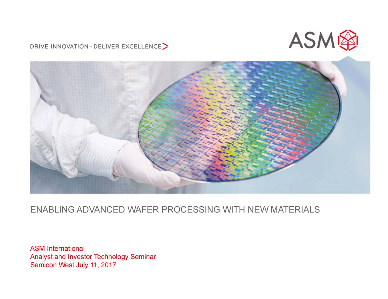
ASM International NV (ASMIY) Investor Presentation - Slideshow

,| ASM International N.V. (ASMIY)
The following slide deck was published by ASM International N.V. in conjunction with a recent investor relations event (SeekingAlpha).

Direct link to pdf-verion at ASM web (LINK)

ASM introduce the Intrepid® ES(TM) 300mm epitaxy tool for logic and memory high-volume production applications

ASM International N.V. (Euronext Amsterdam: ASM) today introduced the Intrepid® ES(TM) 300mm epitaxy (epi) tool for advanced-node CMOS logic and memory high-volume production applications. Intrepid ES introduces innovative closed loop reactor control technology that enables optimal within wafer and wafer-to-wafer process performance, critical for today's advanced transistors and memories. Furthermore, Intrepid ES reduces the cost per wafer significantly for a 7nm epi process compared with prior node processes. The new tool has been qualified for production at a leading-edge foundry customer, and is targeting production applications in other industry segments as well. To date, over 40 reactors have been delivered. 
ASM Epi roadmap as presented at the latest ASMI Analyst and Investor Technology Seminar (www.asm.com)

Tuesday, July 11, 2017

IC Deposition Materials Market Forecast of $1.2B by 2021

Precursors for metals and dielectrics in strong demand for finFETs and 3D-NAND

San Diego, CA, July 11, 2017: TECHCET CA—the advisory service firm providing electronic materials information—today announced that specialty chemical precursor market for the deposition of dielectrics and metals in integrated circuit (IC) fabrication is forecasted to increase at ~10% CAGR through the year 2021. TECHCET’s proprietary Wafer Forecast Model (WFM) shows that 3D-NAND devices are expected to grow at a rapid pace from 2016 and become one of the top three market segments by 2020. Logic ICs will continue to evolve, from 3D finFET devices to Gate-All-Around Nano-Wires (GAA-NW), enabled by new critical materials and manufacturing processes as detailed in new reports from TECHCET, “Advanced Insulating Dielectric Precursors,” and "ALD/CVD High-k & Metal Precursors." 

Precursors tracked by TECHCET for ALD/CVD of metal and high-k dielectric films on IC wafers include sources of aluminum, cobalt, hafnium, tantalum, titanium, tungsten, and zirconium. The total market for 2017 is now estimated to be US$435M, growing to US$638M in 2021. The top-2 suppliers are estimated to hold more than half of the total available market, with many players competing to supply the next enabling molecule. In particular, cobalt precursor demand is forecasted to reach >$80M in 2021 as foundries transition to below 14nm-node processing. As a potential conflict mineral, TECHCET tracks the sub-suppliers of cobalt.

“Metal precursors have had double-digit growth over an extended period of time, and we expect that to continue as the IC industry transitions to 10nm- and 7nm-node logic and 3D-NAND fabrication, with an average long term CAGR of 11% over 2013 to 2021,” says Dr. Jonas Sundqvist, lead author of the report, senior technology analyst with TECHCET and researcher with Fraunhofer IKTS. “Dielectric precursors growth today is clearly driven by dielectric PEALD deposition in multiple patterning, and by dielectric CVD in 3D-NAND.”

Precursors tracked by TECHCET for ALD/CVD/SOD of advanced dielectric films on IC wafers include multiple sources of silicon. The total market for 2017 is now estimated to be just over US$400M, growing to US$560M in 2021. Current growth over 10% is expected to slow slightly to be in the 8-10% range over 2019-2021. Anticipated near-term developments include transitions from CVD to ALD for several IC fab modules.

Global Suppliers of Critical Materials covered in this report include:

Adeka,
Air Liquide,
Dow Corning,
Entegris,
Epivalence,
Fujifilm,
Gelest,
H.C. Starck,
Honeywell,
Kojundo,
Merck EMD,
Nanmat Technology,
Norquay Technology,
Nova-Kem,
Nanogen Solutions,
Pegasus,
Praxair,
STREM,
TCI Chemicals,
Tanaka, 
Tri-Chemical Laboratories,
Umicore,
UP Chemical,
Versum Materials,
Wonik Materials.

Purchase Reports Here: http://techcet.com/product-category/ald-cvd-precursors/http://techcet.com/product-category/ald-cvd-precursors/

ABOUT TECHCET: TECHCET CA LLC is an advisory service firm focused on process materials supply-chains, electronic materials technology, and materials market analysis for the semiconductor, display, solar/PV, and LED industries. Since 2000, the company has been responsible for producing the SEMATECH Critical Material Reports, covering silicon wafers, semiconductor gases, wet chemicals, CMP consumables, Photoresists, and ALD/CVD Precursors. For additional information about these reports or CMC Fabs membership please contact Diane Scott or Michel Walden at info@cmcfabs.org +1-480-332-8336, or go to www.techcet.com or www.cmcfabs.org +1-480-332-8336, or go to www.techcet.com or www.cmcfabs.org


Monday, July 3, 2017

Apple A10X using TSMC 10nm FF has been analyzed by Techinsight

According to reverse engineering by Techinsight, the Apple A10X is confirmed to be built on TSMC’s 10 FF process. The die size is a full node shrink as copared to the previous A9X, which was fabed using the TSMC 16nm FF.

As reported by Techinsight, Samsung was however first on using 10nm for their Samsung Galaxy S8.

Source: Techinsight LINK


Sunday, July 2, 2017

China DRAM startup to enter 19nm chip production in February 2018

DIGITIMES reports that China DRAM startup to enter 19nm chip production in February 2018.

Hefei Rui-Li (transliterated from Chinese) Integrated Circuit will start making DRAM chips using 19nm process technology around the end of February 2018, according to industry sources.

Formerly named Hefei Chang Xin, Rui-Li IC will start installing equipment at its new 12-inch fab at the end of 2017 which is ahead of schedule, said the sources. Rui-Li has started negotiating with silicon wafer providers to ensure a sufficient supply.

Source : DIGITIMES LINK

Toshiba Memory Corporation Announces 96-Layer 3D Flash Memory

TOKYO-Toshiba Memory Corporation, the world leader in memory solutions, today announced that it has developed a prototype sample of 96-layer BiCS FLASH™ three-dimensional (3D) flash memory with a stacked structure*1, with 3-bit-per-cell (triple-level cell, TLC) technology. Samples of the new 96-layer product, which is a 256 gigabit (32 gigabytes) device, are scheduled for release in the second half of 2017 and mass production is targeted for 2018. The new device meets market demands and performance specifications for applications that include enterprise and consumer SSD, smartphones, tablets and memory cards.
 
Source: Toshiba LINK