Wednesday, March 28, 2018

Veeco touts 100 automated MBE systems installed worldwide


Plainview, NY. Veeco Instruments Inc. today announced it has completed installation of its 100th automated Molecular Beam Epitaxy (MBE) system. The installation of Veeco’s GEN10 MBE System last month at Silanna Semiconductor PTY Ltd. in Australia marks this company milestone. The company also operates a Veeco Dual GEN200 MBE System for production of advanced nitride compound semiconductor devices including ultraviolet LEDs (UV-LEDs).

“Veeco has earned a reputation for consistently developing innovative and reliable MBE technology from research scale to production,” said Petar Atanackovic, Ph.D., chief scientist of Silanna Semiconductor PTY Ltd. “The flexibility and deposition capability of the GEN10 system will enable us to develop new materials at the atomic level allowing us to exploit new quantum properties. Veeco’s technology portfolio and leadership in MBE systems provides us with a clear path to easily scale to volume production in the future.”

Source: Evaluation Engineering LINK

Tuesday, March 27, 2018

KLA-Tencor Announces Agreement to Acquire Orbotech Ltd.

[Press release LINK] MILPITAS, Calif., and YAVNE, Israel, March 19, 2018 – KLA-Tencor Corporation (NASDAQ: KLAC) (“KLA-Tencor”) and Orbotech Ltd. (“Orbotech”) today announced they had entered into a definitive agreement pursuant to which KLA-Tencor will acquire Orbotech Ltd. (“Orbotech”) for $38.86 in cash and 0.25 of a share of KLA-Tencor common stock in exchange for each ordinary share of Orbotech, implying a total consideration of approximately $69.02 per share. The transaction values Orbotech at an equity value of approximately $3.4 billion and an enterprise value of $3.2 billion. In addition, KLA-Tencor announced a $2 billion share repurchase authorization. The share repurchase program is targeted to be completed within 12 to 18 months following the close of this transaction.


With this acquisition, KLA-Tencor will significantly diversify its revenue base and add $2.5 billion of addressable market opportunity in the high-growth printed circuit board (“PCB”), flat panel display (“FPD”), packaging, and semiconductor manufacturing areas. The broader portfolio of leading products, services, and solutions, as well as increased exposure to technology megatrends, will support KLA-Tencor’s long-term revenue and earnings growth targets.

Friday, March 23, 2018

ASM International N.V. has published the 2017 annual report

Almere, The Netherlands, March 22, 2018 ASM International N.V. (Euronext Amsterdam: ASM) today publishes its 2017 Annual Report.

ASMI's Annual Report is also available on the company's website www.asm.com. The Annual Report includes the Corporate Responsibility Report and the Remuneration Report in order to increase the relevancy and quality of reporting to all stakeholders.

ASMI will hold its Annual General Meeting of Shareholders (AGM) on May 28, 2018. The AGM agenda with all related documents will be available in due time.

MESSAGE FROM THE CEO (asm.com LINK)
In 2017 we achieved significant progress against our strategic targets. Our sales benefited from a clear recovery in the single-wafer Atomic Layer Deposition (ALD) market, in particular driven by strong increases in the 3D-NAND segment. During the year we also successfully expanded our position in the epitaxy market with an important tool win from a leading foundry customer. In total, our revenue increased by 23% to a new record level. 


Please check out the financial data at a glance here (LINK).

Thursday, March 22, 2018

NCD announced to provide solar cell ALD equipment to SF-PV

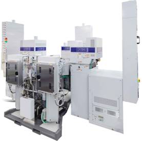
NCD recently shipped the equipment to SF-PV who is a Chinese solar cell manufacturer. This system is (Lucida GS Series + Automation) to increase the efficiency of solar cells by depositing high quality Al2O3 ALD thin films. It will be installed on the site in the end of March and begin production in April.

Lucida GS Series is batch type ALD deposition equipment that forms backside passivation of Al2O3 on multiple wafers and can process more than 4.500 wafers (@ 4nm thickness) of 156mm x 156mm size per an hour. By applying Lucida GS Series in the production of solar cells, customers can dramatically lower the production cost of high efficiency solar cells due to the high-volume productivity, high yield, efficient gas consumption and low maintenance cost compared to competitors. 


(Lucida™ GS series + Automation)

Monday, March 19, 2018

Samsung Electronics Topples Intel to Become World's Largest Chipmaker

The combined share of Samsung Electronics Co. and SK Hynix Inc. in the global semiconductor market stood at 20.7 percent last year, up 5 percent points from a year earlier. Samsung Electronics surpassed Intel as the world's biggest chipmaker by market share for the first time. SK Hynix jumped two spots from the 5th, following Samsung Electronics and Intel.

According to market research firm IHS Markit on March 18, Samsung Electronics’ semiconductor division posted US$62.03 billon (66.28 trillion won) in sales last year, up 53.4 percent from 2016. The company’s market share came to 14.5 percent, exceeding Intel, which had been the world’s biggest seller of chipsets for a long time, by 0.2 percent point. Last year, Intel recorded sales of US$61.46 billion (65.61 trillion won).

SK Hynix, which has become the third largest chip manufacturer, had sales of 26.64 billion (28.46 trillion won) in total last year. Its market share stood at 5.2 percent, followed by Micron Technology Inc. with 5.3 percent, Broadcom Corp. with 4 percent and Qualcomm Incorp. with 3.9 percent

Source: BusinessKorea LINK

Picosun announces significant repeat sales of P-300F batch ALD cluster tools

ESPOO, Finland, 19th March, 2018 – Picosun Group, a leading provider of Atomic Layer Deposition (ALD) thin film coating technology for global industries, reports of significant repeat sales of PICOSUN™ P-300F production cluster tools to major US industry customers.

Semiconductor components manufactured on silicon and compound semiconductor wafers are crucial in several everyday consumer electronics products as well as in e.g. transport, aerospace, or industrial automation and power applications. Even if the majority of the most common IC components is produced on 300 mm silicon wafers, the sub-300-mm manufacturing is vital and increasingly important especially for the existing and emerging non-silicon-based devices. Wafer materials limited to max. 200 mm diameter such as SiC, GaN, AlN, sapphire, GaAs, LiNbO3, and LiTaO3 offer various benefits over silicon and enable a generation of completely new, advanced and innovative end products.
The PICOSUN™ P-300F ALD system is specially designed for production of IC components such as microprocessors, memories, and hard drives, and manufacturing of power electronics, mixed signal, and MEMS devices such as print heads, sensors, and microphones (LINK).

Picosun’s core competence are cost-efficient, turn-key ALD production solutions for the fast growing More-than-Moore market. The PICOSUN™ P-300F tool is the flagship product for these customers. Specially designed to be run in cluster configuration under constant vacuum to enable fast and efficient high throughput manufacturing, the P-300F tools are connected together and operated in fully automatic mode with a central vacuum robot substrate handling and transfer system. The unique batch flipping mechanism in the P-300F tool is ideal for manufacturing lines where the most of the process steps take place in horizontal geometry. Cassette-to-cassette loading for up to 50 pcs batches of 200/150/100 mm wafers, SEMI S2/S8 certification, and SECS/GEM option for factory host integration make the P-300F the optimal choice for demanding manufacturing needs for e.g. moisture barriers, capacitors, and SAW/BAW filters.

“We at Picosun are very happy of the success of our P-300F cluster tools. Our customers have obtained unparalleled process results in them, and this excellent performance has now resulted in repeat sales of these tools to our key industrial customers. The purity, uniformity, and barrier properties of the ALD films deposited in these systems fulfil the strictest requirements of today’s semiconductor industries, making the PICOSUN™ P-300F the tool of choice for the forerunners of semiconductor manufacturing,” states Juhana Kostamo, Managing Director of Picosun.

Sunday, March 18, 2018

Aixtron returned to annual profit in 2017 after sale of ALD/CVD product line

[Semiconductor today] For fourth-quarter 2017, deposition equipment maker Aixtron SE of Herzogenrath, near Aachen, Germany has reported revenue of €54.1m, down 13% on €62.2m last quarter and 39.8% on €89.8m a year ago.

However, full-year revenue was still €230.4m, up 17% on 2016’s €196.5m, and slightly exceeding the guidance of €220-230m. “2017 was a good year for Aixtron, with revenues and orders at the best levels since 2011,” notes VP of finance & administration Charles Russell.

In particular, equipment revenue grew by 21% from €155.7m to €188m (rising from 79% to 82% of total revenue), while sales of spare parts & services rose by just 4% from €40.8m to €42.4m (falling from 21% to 18% of total revenue). 
 
Full article : LINK


Saturday, March 17, 2018

EU suspends review of Linde-Praxair merger, but should resume -Linde

BERLIN, March 15 (Reuters) - German gases group Linde said the European Commission has suspended its review of the group's merger with Praxair while it awaits requested information, but it expects the suspension to be lifted next week.

Source: Reuters LINK

Wednesday, March 14, 2018

MKS has won significant business from a Korean end-user for ALD high flow of ozone systems

Since basically the start of ALD in high volume DRAM manufacturing on 300 mm wafers, ozone has been employed as the co-reactant for ALD of hafnia and zirconia based high-k node dielectrics in the DRAM capacitor memory cell. The ozone concentration directly controls through-put, uniformity and conformalty of the deposited high-k and most importantly also the high-k dielectric performance of the layer including CET/Leakage performance and log term reliability. Please see this early post on details for these processes (LINK)

Just recently MKS Instruments reported (Seeking Alpha Earnings call transcript, LINK) that they won significant business from a Korean end-user for a high flow of ozone systems used in atomic layer deposition to fabricate DRAM memory devices. In addition, MKS reported to have just received a significant suppler award from another major Korean OEM.

MKS further stated that they have made strategic investments with a significant impact on their semiconductor OEM and end-user businesses. Amazingly, the revenue in Korea has increased 250% since 2012. In 2017 alone, their Korea end-user business grew 114%, while the Korea OEM business grew 96%.

Based on this we may assume that high concentration ozone supply i still crucial for the ALD oxide processes in DRAM manufacturing.

MKS Ozone Gas Generators

photo - SEMOZON Ozone Generator

SEMOZON® ozone gas generators and subsystems are the industry standard for compact, high concentration, ultra-clean ozone gas generation. Applications include Atomic Layer Depostion (ALD), Chemical Vapor Deposition (CVD), cleaning and water treatment.

Link to MKS Instrument Ozone products: LINK

MKS Instruments, Inc. is a global provider of instruments, subsystems and process control solutions that measure, control, power, monitor, and analyze critical parameters of advanced manufacturing processes to improve process performance and productivity.  The Company’s products are derived from core competencies in pressure measurement and control, flow measurement and control, gas and vapor delivery, gas composition analysis, residual gas analysis, leak detection, control technology, ozone generation and delivery, RF & DC power, reactive gas generation, vacuum technology, lasers, photonics, sub-micron positioning, vibration isolation, and optics.  MKS’ primary markets include semiconductor capital equipment, general industrial, life sciences, and research.  Additional information can be found at www.mksinst.com.

Tuesday, March 13, 2018

AMEC introduces ICP Etch for memory and logic at SEMICON China

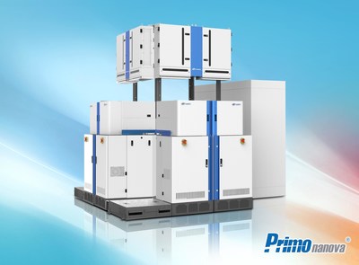
SHANGHAI, March 12, 2018 /PRNewswire/ -- This week at SEMICON China, Advanced Micro-Fabrication Equipment Inc. (AMEC) formally unveiled the Primo nanova® system (nanova) - the company's first inductively coupled plasma (ICP) etcher for high-volume front-end production of memory and logic ICs. The system combines proprietary ICP technology innovations and novel features to help customers achieve application imperatives like tight critical dimension (CD) uniformity and superior control. Key differentiations include a specialized symmetric chamber configuration that enables very high pumping speed, as well as a novel low-capacitive coupling coil design, and a temperature-controlled multiple-zone electrostatic chuck (ESC). With these and other unique features, the system delivers superior process performance for critical conductor and dielectric etch applications at device nodes of 5nm and below, at a cost of ownership (CoO) that is significantly lower than comparative tools.

AMEC has received orders for the nanova system from multiple customers. Products have been shipped and the first tool is already in production and demonstrating very stable yield. The company is now accelerating demo requests. The system strengthens AMEC's portfolio of etch tools which includes multi-generation capacitively coupled plasma (CCP) dielectric and TSV etch product families.

The nanova system was engineered to address today's IC manufacturing complexities where new materials, new transistor structures, double and even quadruple patterning, and other technology advancements are helping to ensure continued device shrinks. Critical success imperatives for etch in this processing environment are high uniformity and superior control across the wafer, with wide process window. The nanova system meets these technical requirements in a cost-effective single-station chamber tool.

"The nanova system deploys today's most advanced etch technology to empower customers at the leading edge with enabling innovation and exceptional flexibility," said Dr. Tom Ni, VP and GM of AMEC's Etch Product Business Group. "The system can process diverse conductor etch applications, like STI, poly-gate, spacer, mask etching and etch-back, with industry-leading productivity and superior on-wafer performance. As an ICP-based technology, it can etch deep vertical holes, as well as shallow tapered features. It's a cost-competitive solution as well, thanks to a smaller-than-average footprint and an innovative design that reduces consumables use. We're excited to see customers already benefiting from the tool."


Monday, March 12, 2018

SoLayTec ships new ALD order to Asia for PERC cell manufacturing

North American Clean Energy reports (LINK): Amtech Systems, Inc. (NASDAQ: ASYS), a global supplier of production equipment and related supplies for the solar, semiconductor, and LED markets, announced its solar subsidiary, SoLayTec B.V., has shipped a next generation solar Atomic Layer Deposition (ALD) to an Asian customer. While the PV market is shifting towards high efficiency cell designs, production with high yield, A-grade cells, is getting increasingly important.

Fokko Pentinga, CEO and President of Amtech, commented, "For this project we are delivering the equipment for the PERC line upgrade and assisting the customer with the PERC ramp-up and line integration. PV manufacturers are experiencing extreme price pressure, resulting in an increasing need for higher cell quality with narrow cell efficiency distribution. The highest line yield possible of A-grade cells is essential to ensure good margins for these advanced production lines. Al2O3 wrap-around during deposition will result in reduction of the cell efficiency by as much as 0.2%, as well as front side color variations. Our ALD equipment addresses PV manufacturers' challenges, by delivering the highest PERC cell efficiency using Al2O3,, highest A-grade cells, and stable deposition process without any wrap around. Another challenge we address for A-grade cells is scratch free manufacturing of SiNx deposition for rear-side capping and front-side ARC. Our scratch free solution using our direct-plasma PECVD equipment is gaining momentum, with shipments and order backlog totaling more than 1GW."

Tuesday, March 6, 2018

Applied Materials see high growth for Display business >30% growth

Applied Materials, Inc. (AMAT) recently reported record revenue and operating profit in its first quarter ended January 28, 2018. Besides beeing the big giant for wafer equipment they are also in the lead for display, for TV as well as smartphone and especially for the lastets size 10.5 Gen.

According the the recent news covered by Seeking Alpha (LINK), Applied Materials is counting on revenue growth from 10.5G LCD plants and from its operations in LTPS backplanes and OLED encapsulation, primarily for the smartphone sector.

In the recent 1Q 2018 earnings call - Gary E. Dickerson - Applied Materials said: "In Display, there are two equally large market inflections driving capital investments: the introduction of Gen 10.5 substrates for TV manufacturing and organic LED displays. In mobile, the transition to OLED displays is compelling. This is because rigid OLED offers significant performance, power and cost advantages over LCD, and flexible OLED will enable new form factors, such as curved and eventually foldable screens. As a result, our positive outlook for 2018 and beyond remains unchanged. Display is a unique growth driver for Applied, and we expect to increase our revenue by more than 30% in 2018 on top of nearly 60% growth last year."
Dickerson further stated:
  • year-over-yearoutlook for Display business is greater than 30% growth, and 2019 and beyond also look very strong.
  • for mobile versus TV Applied Materials has an about 50/50 mix. In TV, they see increased adoption of larger screens and they are tracking 13 Gen 10.5 projects. As an example if you produce 65-inch TVs with Gen 10.5, you get eight 65-inch TVs per plane and only three with Gen 8.5 and driving the TV business.

Chart above from IHS (thru SeekingAlpha, LINK) shows planned equipment purchases for 10.5G quipment, install dates, and production ramp up.


Applied Materials AKT-PECVD covers the complete range of glass sizes used in the display industry from Gen 2 (0.2m2) all the way up to Gen 10 (9m2). The systems offer processes for both amorphous silicon (a-Si) and metal oxide (MOx) backplane technologies. Available films include both doped and undoped (a-Si), silicon oxide (SiOx), silicon oxynitride (SiON), silicon nitride (SiN), and in-situ multi-layer deposition. (appliedmaterials.com)
According to Seeking Alpha the maine cometitors for current technologies (<10.5 Gen) are :
For the TFT Backplane:
  • PECVD companies - AMAT, Jusung Engineering (Korea), and Wonik IPS (Korea)
  • PVD companies - AMAT, Avaco (Korea), Iruja (Korea), and Ulvac (Japan)
  • Laser Anneal companies – Coherent, AP Systems (Korea), Japan Steel Works (Japan)
For the OLED Encapsulation:
  • Jusung Engineering (Korea)
  • Wonik IPS (Korea)
  • TES (Korea)
These Korean companies all have ALD technologies and equipment for displays. The advantages with ALD are:
  • thin films offer better water and oxygen protection
  • a thinner film is needed to provide the same protection as thicker PECVD-coated films
  • the slower coating process by ALD is compensated by a thinner film 

Monday, March 5, 2018

OIPT delivers record number of integrated ‘Lab to Fab’ solutions

[Semiconductor Today] UK-based plasma etch and deposition processing system maker Oxford Instruments Plasma Technology (OIPT) is celebrating a year of delivering a record number of integrated solutions, enabling customers to rapidly commercialize semiconductor devices, developed using Oxford Instruments ‘Lab to Fab’ solutions.

Oxford Instruments says that many of its customers are now converting their research into commercially available devices. The key to success is to transfer the results achieved in development and pilot facilities, and repeat them every day, every month in the fabrication facility, notes the firm. OIPT reckons that, due to its installed base of R&D tools, it is ideally placed to offer this ‘Lab to Fab’ solution. 
 
“We’ve shipped over 600 of our high-technology process modules to leading production facilities and, with an increasing demand from the optoelectronics, power and other leading markets, our plasma process solutions are being utilized globally to achieve excellent device performance and throughput,” says OIPT’s sales & marketing director Paul Davies.
 
Semiconductor Today LINK


Sunday, March 4, 2018

Major suppliers have improved their 3D NAND production yield rates

Revenues of the global NAND flash industry grew only 6.8% sequentially in the fourth quarter of 2017, according to DRAMeXchange. Traditionally seasonal factors will continue to influence sales in the first quarter of 2018.

Major suppliers have improved their 3D NAND production yield rates at a gradual pace, said DRAMeXchange. On the demand side, the smartphone market entered its peak season in the fourth quarter resulting in an up to 5% sequential rise in contract prices for eMMC and UFS devices.

However, demand for PCs, tablets and servers slowed down in the fourth quarter with contract prices for related NAND flash chips stayed flat or slipped on quarter, DRAMeXchange indicated. As a result, the overall NAND flash market shifted toward an equilibrium of supply and demand in the fourth quarter of 2017,

The NAND flash market has seen a slight oversupply in the first quarter of 2018, due to a generally seasonal slowdown in end-market demand, according to DRAMeXchange. The chip suppliers will likely post revenue decreases as they cut prices to spur demand, but will be able to maintain a healthy level of profits thanks to their transitions to 64- and 72-layer 3D NAND technologies.
 
Source: DIGITIMES LINK
 

China to Join Hands with Intel to Develop 3D NAND against Korea

China-Intel AllianceChina's Tsinghua Unigroup is cooperating with Intel Corp. to develop 3D NAND flash memory chips in earnest. Tsinghua Unigroup supported by the Chinese government's huge amount of capital is joining forces with Intel which has technology in memory chips.
 

Presentation Intel 3D NAND from Intel: Bringing Amazing SSDs to the Mainstream (LINK)
 
According to DRAMeXchange and industry sources on March 2, China’s Tsinghua Unigroup and Intel are discussing how to work together to develop and produce 3D NAND technologies in the long term.


DRAMeXchange released its report on the 1st, saying, “According to the contract, Intel has decided to deliver wafers for NAND flash chips first before supplying 64-layer 3D NAND flash chips. With Intel’s support, Tsinghua Unigroup’s products will be able to improve not only its competitiveness in sales but also its brand awareness in the market.”

Tsinghua Unigroup and Intel are leaders that can create a remarkable synergy of capital and technology. Tsinghua Unigroup is the biggest beneficiary of the Chinese government’s plan to invest 1 trillion yuan (US$157.53 billion or 170.61 trillion won) in order to raise its semiconductor self-sufficiency rate to 70 percent by 2025. Tsinghua Unigroup’s NAND plant, which has been constructed with the investment of 26 trillion won (US$24.01 billion), will start manufacturing 32-layer 3D NAND flash chips from the end of this year and expand the facilities to significantly increase the production next year. 
 
Source: BusinessKorea  LINK

Thursday, March 1, 2018

China Is Raising Up to $31.5 Billion to Fuel Chip Vision

[Bloomberg, LINK] China’s government aims to raise as much as 200 billion yuan ($31.5 billion) to invest in homegrown chip companies and accelerate its ambition of building a world-class semiconductor industry, people familiar with the matter said.

The state-backed China Integrated Circuit Industry Investment Fund Co. is in talks with government agencies and corporations to raise at least 150 billion yuan for its second fund vehicle but is angling for up to 200 billion yuan, the people said, asking not to be identified talking about a plan that hasn’t been publicized. It intends to begin deploying capital in the second half of the year, they added.

The firm will again invest in a wide range of sectors from processor design and manufacturing to chip testing and packaging, potentially benefiting industry leaders from telecoms gear makers Huawei Technologies Co. and ZTE Corp. to major players such as the Tsinghua Group. The first fund -- about 140 billion yuan -- had gone toward more than 20 listed companies, including ZTE and contract chipmaker Semiconductor Manufacturing International Corp., the people said.

Smaller chip players gained in the afternoon. Integrated circuit manufacturer Jiangsu Changjiang Electronics Technology Co. climbed as much as 6.2 percent in afternoon trading in Shanghai, while chip packager China Wafer Level CSP Co. gained almost 5 percent.
 
The figure above illustrates the projected top spenders in China from 2016 to 2020. SMIC will lead the pack in fab equipment investment with its new 300mm fab projects in Beijing, Shanghai, and Shenzhen as well as 200mm investment in Tianjin.  However, the number two to number five positions are all occupied by multinationals, especially from the memory segment. Samsung will continue its phase two investment in Xian; Intel is ramping up its 3D NAND capacity in Dalian; and SK Hynix is building a new DRAM fab in Wuxi. New memory players in China will only start to increase spending in the latter half of the forecast period. Aggressive investment is also planned by leading foundries in China including GLOBALFFOUNDRIES’ Chengdu fab, Hua Li Micro’s Fab 2 in Shanghai, UMC’s Xiamen fab, and TSMC’s Nanjing fab. Compared to a year ago, the investment levels and schedules of multinational companies’ in China have become more aggressive. [SEMI, LINK]

2017 was a year of recovery in ALD business driven by 3DNAND according to ASMI

Today was the ASM International NV (OTCQX:ASMIY) Q4 2017 Earnings Conference Call for analysts. The call has been transcripeted by Seeking Alpha (LINK). All in all 2017 was a good year for ALD single wafer market and showed recovery from 2016.  Here is some important take aways from Peter van Bommel - CFO, during teh call:


  • Looking at the company's financial performance, 2017 was a year of recovery in our ALD business. In particular, driven by strong increases in the 3D NAND segment. 2017, we also successfully increased our addressable market in epitaxy as we rolled our first leading high volume manufacturing customer for our new Intrepid too. Initial cost related to new product launches impacted to the gross margin but we still increased our operating profits by 38% in 2017.
  • In terms of product lines, the key driver was our ALD business, at some distance followed, by Epi and PECVD. Our net sales in 2017 increased by 23% to a new record high of €737 million. Sales were led by our ALD product line, which continued to represent clearly more than half of our equipment revenue.


ASM earnings call slide (sceeen dump from Seeking Alpha LINK)


  • By industry segment, the revenue stream in the fourth quarter was led by memory customers, largely 3D NAND, followed by foundry. Looking at the roadmaps of our customers, the introduction of complex 3D devices structures and new materials and further scaling, will drive the need for more precise deposition of ultrathin and highly comfortable films. This place is the strength of ALD. And as a leader in the single wave of ALD market, our company remains well-positioned to capture the growth expected in this market.

Looking ahead the addressable market for single wafer ALD will grow according to Peter van Bommel since the advanced node share  (14, 10 and 7 nm) will grow to roughly 50% in revenue by 2020-2021 of the total wafer fab equipment spending, when ASM expect the single wafer ALD market to reach  USD 1.5 billion annual revenue (see graph below, Gartner Dec 2017).


ASM earnings call slide (sceeen dump from Seeking Alpha LINK

Not touched upon too much was the Large Batch furnace segment which is dominated by the competitors Tokyo Electron and Hitachi Kokusai. This segment is however much smaller than the single wafer ALD segement, maybe 70:30 ratio or so. The patent disagreement with the Hitachi Kokusai was briefly mentioned but nothing substantial was said since it is an ongoing issue (LINK).