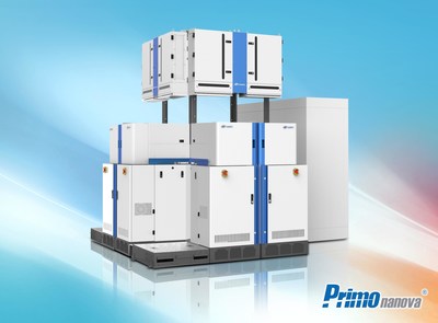
SHANGHAI, March 12, 2018 /PRNewswire/ -- This week at SEMICON China, Advanced Micro-Fabrication Equipment Inc. (AMEC) formally unveiled the Primo nanova® system (nanova) - the company's first inductively coupled plasma (ICP) etcher for high-volume front-end production of memory and logic ICs. The system combines proprietary ICP technology innovations and novel features to help customers achieve application imperatives like tight critical dimension (CD) uniformity and superior control. Key differentiations include a specialized symmetric chamber configuration that enables very high pumping speed, as well as a novel low-capacitive coupling coil design, and a temperature-controlled multiple-zone electrostatic chuck (ESC). With these and other unique features, the system delivers superior process performance for critical conductor and dielectric etch applications at device nodes of 5nm and below, at a cost of ownership (CoO) that is significantly lower than comparative tools.
AMEC has received orders for the nanova system from multiple customers. Products have been shipped and the first tool is already in production and demonstrating very stable yield. The company is now accelerating demo requests. The system strengthens AMEC's portfolio of etch tools which includes multi-generation capacitively coupled plasma (CCP) dielectric and TSV etch product families.
The nanova system was engineered to address today's IC manufacturing complexities where new materials, new transistor structures, double and even quadruple patterning, and other technology advancements are helping to ensure continued device shrinks. Critical success imperatives for etch in this processing environment are high uniformity and superior control across the wafer, with wide process window. The nanova system meets these technical requirements in a cost-effective single-station chamber tool.
"The nanova system deploys today's most advanced etch technology to empower customers at the leading edge with enabling innovation and exceptional flexibility," said Dr. Tom Ni, VP and GM of AMEC's Etch Product Business Group. "The system can process diverse conductor etch applications, like STI, poly-gate, spacer, mask etching and etch-back, with industry-leading productivity and superior on-wafer performance. As an ICP-based technology, it can etch deep vertical holes, as well as shallow tapered features. It's a cost-competitive solution as well, thanks to a smaller-than-average footprint and an innovative design that reduces consumables use. We're excited to see customers already benefiting from the tool."

The Primo nanova System: Key Enabling Attributes and Advantages
The six-chamber tool with two load lock strippers features proprietary innovations that collectively enable higher productivity and greater throughput. They include:
- A proprietary low-capacitive coupling coil design that enables more independent ion density and energy which is essential for higher selectivity and soft etch;
- A symmetric chamber design featuring a multi-zone ESC and active-edge tilting control for better uniformity. AMEC engineered the design to overcome side-to-side non-uniformity which has been a persistent challenge in high-volume manufacturing;
- Wide process window and precise localized profile control with significantly higher pumping speed when compared to similar products;
- Innovative plasma-enhanced PVD coating, coupled with precise chamber wall temperature and superior chamber environment control for greater process stability and defect reduction.
Dr. Ni further noted: "Feedback from customers confirms that the nanova system delivers the on-wafer performance and productivity we intended, and with compelling CoO benefits. It's a flexible tool that is equipped to process diverse applications with minimal configuration adjustments."
No comments:
Post a Comment