Friday, November 30, 2018

Gooch & Housego Installs Veeco’s IBS System for Advanced Optical Coating Capabilities


PLAINVIEW, New York—Nov. 29, 2018—Veeco Instruments Inc. and Gooch & Housego (G&H), the world’s leading supplier of high quality superpolished optical components today announced the successful installation of Veeco’s SPECTOR® Ion Beam Sputtering (IBS) Optical Coating System at G&H’s Moorpark, Calif. facility. The new capability provided by SPECTOR supports G&H’s expanding portfolio of high-quality optics for ultraviolet, visible and infrared systems used in telecommunications, aerospace and defense, life science and industrial applications.

SPECTOR offers exceptional layer thickness control, enhanced process stability and the lowest published optical losses in the industry, and has become the IBS system of choice for over 200 advanced manufacturing settings worldwide. G&H will use this system to support its expanding portfolio of high-quality optics for UV, visible and infrared systems used across telecommunications, aerospace and defense, life science and industrial applications. 
 
“G&H is at the forefront of engineering a broad range of photonics technologies, leveraging optical coatings to advance crystal growth, electro-optics and fiber optics in next-generation applications,” said Adam Morrow, product line manager at G&H. “As we navigate the increasingly complex specifications required for these processes, we’ve turned to Veeco as a partner that can uphold our long-standing pedigree of high-quality optics.”

G&H’s growing presence in the laser optics landscape builds on the company’s tenured history as a supplier of high-quality photonics components. Complementing G&H’s superpolished surfaces, Veeco offers IBS coatings that achieve very low levels of total loss while maintaining surface roughness quality, density and exceptional environmental stability.


The SPECTOR IBS platform offers exceptional layer thickness control, enhanced process stability, and the lowest published optical losses in the industry. The system is engineered to improve key production parameters, such as target material utilization, optical endpoint control, and process time for cutting-edge optical coating applications. The SPECTOR platform, which is the preferred IBS system in the industry, has been installed in more than 200 advanced manufacturing settings across the world.


“Veeco’s IBS systems allow our customers to achieve the highest precision and thin film process flexibility necessary for successful advanced photonics and next-generation high-growth applications,” added Adrian Devasahayam, Ph.D., vice president and general manager of Veeco’s Advanced Deposition and Etch (AD&E) business. “We’re confident in the SPECTOR system’s ability to provide G&H with the qualitative advantages of IBS technology, including low scatter loss, high film purity, stable deposition rates and film thickness control of less than 0.1 nm in a robust package that significantly boosts throughput and lowers cost of ownership for customers.”


According to BCC Research, the global market for optical coatings is expected to reach $14.2 billion in 2021, up from $9.5 billion in 2016. Key drivers of this growth are emerging applications in commercial and consumer categories, as well as innovative coatings to improve a broad range of existing applications.

GLOBALFOUNDRIES announces industry’s first 300 mm SiGe foundry technology

GLOBALFOUNDRIES Announces Industry’s First 300mm SiGe Foundry Technology to Meet Growing Data Center and High-Speed Wireless Demands

Santa Clara, Calif., November 29, 2018 – GLOBALFOUNDRIES today announced its advanced silicon germanium (SiGe) offering, 9HP, is now available for prototyping on the company’s 300mm wafer manufacturing platform. The move signifies the strong growth in data center and high-speed wired/wireless applications that can leverage the scale advantages of a 300mm manufacturing footprint. By tapping into GF’s 300mm manufacturing expertise, clients can take advantage of increased production efficiency and reproducibility for high-speed applications such as optical networks, 5G millimeter-wave wireless communications and automotive radar.


Globalfoundries Fab 10 in East Fishkill, NY
 
GF is the industry leader in the manufacturing of high-performance SiGe solutions on its 200mm production line in Burlington, Vermont. The migration of 9HP, a 90nm SiGe process, to 300mm wafers manufactured at GF’s Fab 10 facility in East Fishkill, N.Y., continues this leadership and establishes a 300mm foothold for further roadmap development, ensuring continued technology performance enhancements and scaling.
“The increasing complexity and performance demands of high-bandwidth communication systems have created the need for higher performance silicon solutions,” said Christine Dunbar, vice president of RF business unit at GF. “GF’s 9HP is specifically designed to provide outstanding performance, and in 300mm manufacturing will support our client’s requirements for high-speed wired and wireless components that will shape future data communications.”

GF’s 9HP extends a rich history of high-performance SiGe BiCMOS technologies designed to support the massive growth in extremely high data rates at microwave and millimeter-wave frequencies for the next generation of wireless networks and communications infrastructure, such as terabit-level optical networks, 5G mmWave and satellite communications (SATCOM) and instrumentation and defense systems. The technology offers superior low-current/high-frequency performance with improved heterojunction bipolar transistor (HBT) performance and up to a 35 percent increase in maximum oscillation frequency (Fmax) to 370GHz compared to its predecessors, SiGe 8XP and 8HP.

Client prototyping of 9HP on 300mm at Fab 10 in East Fishkill, N.Y. on multi-project wafers (MPWs) is underway now, with qualified process and design kits scheduled in 2Q 2019.

For more information on GF’s SiGe solutions, contact your GLOBALFOUNDRIES sales representative or visit globalfoundries.com.

Tuesday, November 27, 2018

Globalfoundries Fab 11 will ramp straight on to 22nm FD-SOI process for Chinese customers

[Andantech] Fab 11 was/is built as a partnership between GlobalFoundries and the Chengdu municipality. The original plan for the Chengdu fab included two phases with an aggregated capacity of approximately 1,000,000 wafers per year when both operate at full capacity. The first phase was to start operations in 2018 and process around 20,000 wafers per month using mainstream 180/130 nm fabrication technologies originally developed by Chartered for various general-purpose chips. The second phase was to begin operations in 2019, use GlobalFoundries’ 22FDX process and gradually expand its capacity to 65,000 wafers per month. At the same time, one of the terms of the agreement between GF and the Chengdu municipality was to develop an FD-SOI ecosystem locally.
 
 
Based on various reports, GlobalFoundries has failed to land orders for chips to be made using bulk 180/130 nm fabrication processes. As a result, the company will not equip its Fab 11 for those processes, but instead will jump straight to 22FDX. So far, GlobalFoundries has landed orders from six customers in China for 22FDX chips and these clients are currently ramping up their wafers at Fab 1 in Dresden, Germany.

“Given GlobalFoundries' renewed focus on differentiated offerings and discussions with potential clients, we have decided to bypass the original phase-one investment in mainstream process technology,” a GlobalFoundries executive said in an interview with DigiTimes. “In order to meet demand from China for differentiated offerings including our 22FDX technology, we have to revise the original timeline in order to better align capacity.”
 
Source: Andantech LINK


Monday, November 26, 2018

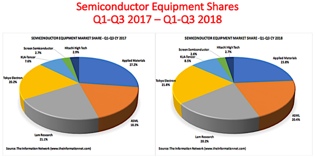
Applied Materials is getting closer to losing its dominance in the Semiconductor Equipment market

According to Seeking Alpha, Applied Materials is getting closer to losing its dominance in the Semiconductor Equipment market
  • Applied Materials recently reported semiconductor equipment revenue growth dropped 16.0% compared to the previous quarter due largely to pushouts in equipment by memory customers.
  • Applied Materials has been losing market share to competitor Tokyo Electron since 2017 and is close to losing its long-held title of semiconductor equipment leader.
  • 60% of Applied Materials revenues was due to purchased by memory companies, but DRAM and NAND capex spend is projected to drop in 2018 and 2019.
 
 
Source: Seekeing Alpha LINK

Friday, November 23, 2018

Top-3 memory chipmakers combined DRAM revenues hit record high in 3Q/201818

The world's top-3 memory IC vendors - Samsung Electronics, SK Hynix and Micron Technology - saw their combined DRAM and flash memory revenues climb to a record high of US$37.3 billion in the third quarter of 2018.


The combined revenues for third-quarter 2018 represented increases of 8% sequentially and 36% on year, thanks mainly to demand for servers and smartphones that come with higher density memory specs.

DRAM chip sales accounted for as high as 71% of the combined memory chip revenues generated by the top-3 vendors in the third quarter of 2018, Digitimes Research indicated. The top-3 memory chip vendors saw their combined DRAM memory sales reach US$26.4 billion in the third quarter, up 10% sequentially.


Source: DIGITIMES LINK

Thursday, November 22, 2018

Picosun Group reports significant increase in turnover and profitability


ESPOO, Finland, 23rd November 2018 – Picosun Group, a leading provider of advanced ALD (Atomic Layer Deposition) thin film coating technology for global industries, reports 37 % rise in turnover to 25.96 million euros during its previous fiscal year, which ended 30th September 2018. 

 
At the same time, the company increased its profitability. EBIT grew to 1.42 million euros which equals 5.5 % of turnover, and EBITDA to 2.39 million euros which is 9.2 % of turnover. The numbers are still unconfirmed.

Picosun’s personnel grew one third to 86 people. Almost 25 % of the personnel have either Ph.D. or D.Sc. degree.

”We are very pleased with the numbers of the previous fiscal year. What also makes us happy is the fact that we were able to increase important investments that support development of our company. Agility and unmatched ALD expertise are our core strengths which we will never compromise,” says Mr. Kustaa Poutiainen, Chairman of the Board and CEO of Picosun Group.

Last year, Picosun invested 4.4 million euros to research and development. This is 17 % of the company’s turnover.

For the ongoing fiscal year Picosun has budgeted 33.3 million euros turnover, which means 28 % growth. The company is also expecting further improvement in profitability, and it is planning to increase its R&D investments to 5.7 million euros.

Picosun’s personnel is expected to grow at the same rate as during the previous fiscal year. Healthcare business will be one of the key factors to boost Picosun’s growth.

”Our PicoMEDICAL™ solutions, specifically targeted to the healthcare industries, have raised a lot of interest amongst our customers. ALD will revolutionize advanced health technologies, just like it did to microelectronics industries more than ten years ago. As the leading AGILE ALD™ solutions provider, we are the pioneers in this field,” continues Poutiainen.

The company has strengthened its global Service and Support operations by hiring lots of new personnel, and by establishing a specific Customer Experience unit. Also Picosun’s China operations have undergone restructuring, and they shall be significantly reinforced during the ongoing fiscal year.

Picosun provides the most advanced ALD thin film coating technology to enable the industrial leap into the future, with turn-key production solutions and unmatched expertise in the field. Today, PICOSUN™ ALD equipment are in daily manufacturing use in numerous major industries around the world. Picosun is based in Finland, with subsidiaries in Europe, North America, Singapore, Taiwan, China, and Japan, and a world-wide sales and support network. Visit www.picosun.com.

Wednesday, November 21, 2018

China's InnoScience orders Aixtron AIX G5+ C MOCVD systems for manufacturing 650V GaN-on-Si devices

 
Deposition equipment maker Aixtron SE of Herzogenrath, near Aachen, Germany is to deliver multiple AIX G5+ C MOCVD systems to China's InnoScience Technology Co Ltd for the development of gallium nitride (GaN) power devices, which are increasingly favored over silicon power devices due to their superior performance at high frequency. All Aixtron cluster tools will feature a 5x200mm-wafer configuration and will be shipped by second-quarter 2019.
 
Source: Semiconductor Today LINK

Monday, November 19, 2018

TSMC to supply IBM with data center chips challenging Intel's dominance


Taiwan Semiconductor Manufacturing Company (TSMC) is set to sign a deal with IBM to produce mainframe server chips. As a big player in the global data center market, a contract to supply IBM could propel TSMC into a position to contend with Intel which currently owns the market.

The business machine giant designs its own server chips, which are presently produced by GlobalFoundries, so the change to a new supplier is a big blow for the rival manufacturer. According to sources with Nikkei, IBM looks to move to a smaller process for its next generation of mainframe servers, and Taiwan-based TSMC has the only 7nm technology available.

Source: TechSpot (LINK)

Friday, November 16, 2018

New Applied Materials META Center at SUNY Albany

SANTA CLARA, Calif., Nov. 15, 2018 (GLOBE NEWSWIRE) -- Applied Materials, Inc. today announced plans for the Materials Engineering Technology Accelerator (META Center), a major expansion of the company’s R&D capabilities aimed at creating new ways for Applied and its customers to drive innovation as classic Moore’s Law scaling becomes more challenging. 

Applied Materials engineers work on the latest technology to help enable faster, more efficient microchips (Applied Materials, Inc.)
The primary goal of the META Center is to speed customer availability of new chipmaking materials and process technologies that enable breakthroughs in semiconductor performance, power and cost. The new center will complement and extend the capabilities of Applied’s Maydan Technology Center in Silicon Valley.

The META Center will be a hub for innovation, delivering on a call to action by Applied CEO Gary Dickerson for increased collaboration and speed across the technology ecosystem.

“Realizing the full potential of Artificial Intelligence and Big Data will require significant improvements in performance, power consumption and cost both at the edge and in the cloud,” said Gary Dickerson, president and CEO of Applied Materials. “The industry needs new computing architectures and chips enabled by innovative materials and scaling approaches. The META Center creates a new platform for working with customers to accelerate innovation from materials to systems.” 

Albany Campus (SUNY Albany)
Scheduled to open in 2019, the META Center will be a first-of-its kind facility, spanning 24,000 square feet of cleanroom. It will be furnished with a broad suite of Applied’s most advanced process systems along with complementary technologies needed for new chip materials and structures to be piloted for high-volume production at customer sites.

To be located at the State University of New York Polytechnic Institute (SUNY Poly) campus in Albany, New York, the META Center will be created under agreements to be entered into with New York State, The Research Foundation for The State University of New York and SUNY Poly, that have been approved by the Empire State Development Board of Directors and are subject to further approval by The New York State Public Authorities Control Board.


“SUNY Poly provides an ideal combination of infrastructure, capabilities and talent in a thriving academic and entrepreneurial setting with deep roots in the semiconductor industry,” said Steve Ghanayem, senior vice president of New Markets and Alliances at Applied Materials. “The technology ecosystem will benefit from the acceleration of materials innovation through collaboration at the META Center.”

Wednesday, November 14, 2018

SK Hynix : Announces 1Ynm 16Gb DDR5 DRAM


(marketscreener.com) SK Hynix Inc. Announces 1Ynm 16Gb DDR5 DRAM2018.11.15 Seoul, November 15, 2018 - SK Hynix Inc. (or 'the Company', www.skhynix.com) announced that it has developed 16Gb (Gigabits) DDR5 (Double Data Rate 5) DRAM, the industry's first DDR5 to meet the JEDEC standards. 
 
The same 1Ynm process technology used for the recently-developed 1Ynm 8Gb DDR4 DRAM was applied to the new DRAM, giving an industry-leading competitive edge for the Company. DDR5 is a next-generation DRAM standard that offers ultra-high speed and high density with reduced power consumption as compared to DDR4, for use in data-intensive applications such as big data, artificial intelligence, and machine learning. SK Hynix successfully lowered the operating voltage from 1.2V to 1.1V, achieving 30% lower power consumption compared to the previous generation, DDR4 DRAM. The new 16Gb DDR5 DRAM supports a data transfer rate of 5200Mbps, about 60% faster compared to 3200Mbps of the previous generation, with which it can process 41.6GB (Gigabytes) of data-11 full-HD video files (3.7GB each)-per second. The Company provided a major chipset maker with RDIMM (Registered Dual In-line Memory Module) and UDIMM (Unbuffered DIMM) for server and PC platforms, with more memory banks-doubled from 16 to 32 banks-in accordance with the JEDEC DDR5 standards. 'Based on technological advancements that allowed the industry's first DDR5 DRAM to meet the JEDEC standards, SK Hynix plans to begin mass producing the product from 2020, when the DDR5 market is expected to open, to actively respond to the demands of clients,' said vice president Joohwan Cho, the Head of Volume Product Design Group. According to IDC, a market research institute, demand for DDR5 is expected to rise from 2020, accounting for 25% of the total DRAM market in 2021 and 44% in 2022.

Source: 4-traders LINK

EpiGaN Increases Production with AIXTRON's MOCVD Equipment


EpiGaN, the Belgian GaN-on-Si and GaN-on-SiC epitaxial wafer provider, has ordered a new AIX G5+ C system from AIXTRON to expand its production capability for large size wafer.
 
The new AIXTRON AIX G5+ C reactor will be installed at EpiGaN’s manufacturing site in Hasselt Belgium in the first quarter of 2019 and start to operate afterwards. The fully automated Planetary® MOCVD system features in-situ chamber cleaning and enables configurations of 8x6 inch or 5x8 inch epitaxial wafers to be automatically loaded and removed by a cassette-to-cassette wafer transfer module.

Source: LEDinside LINK

Tuesday, November 13, 2018

Spin Memory Teams With Applied Materials to Produce a Comprehensive Embedded MRAM Solution

FREMONT, Calif. — Spin Memory, Inc. (Spin Memory), the leading MRAM developer, today announced a commercial agreement with Applied Materials, Inc. (Applied) to create a comprehensive embedded MRAM solution. The solution brings together Applied’s industry-leading deposition and etch capabilities with Spin Memory’s MRAM process IP.


Key elements of the offering include Applied innovations in PVD and etch process technology, Spin Memory’s revolutionary Precessional Spin CurrentTM (PSCTM) structure (also known as the Spin Polarizer), and industry-leading perpendicular magnetic tunnel junction (pMTJ) technology from both companies. The solution is designed to allow customers to quickly bring up an embedded MRAM manufacturing module and start producing world-class MRAM-enabled products for both non-volatile (flash-like) and SRAM-replacement applications. Spin Memory intends to make the solution commercially available from 2019.

“In the AI and IoT era, the industry needs high-speed, area-efficient non-volatile memory like never before,” said Tom Sparkman, CEO at Spin Memory. “Through our collaboration with Applied Materials, we will bring the next generation of STT-MRAM to market and address this growing need for alternative memory solutions.”

“Our industry is driving a new wave of computing that will result in billions of sensors and a dramatic increase in data generation,” said Steve Ghanayem, senior vice president of New Markets and Alliances at Applied Materials. “As a result, we are seeing a renaissance in hardware innovation, from materials to systems, and we are excited to be teaming up with Spin Memory to help accelerate the availability of a new memory.”
About the PSC

Updated website NCD for ALD technology and equipment

Updated website NCD for ALD technology and equipment: www.ncdtech.co.kr

NCD updated its website with re-formation and company promotional video clip for the introduction and main equipment.